- When Write = 0, the output of the 1-bit memory will not change (eventhough the input value to the 1-bit memory may change - the memory must remember the store value, i.e., the output must remain the same because the output of the memory represents the value stored inside the memory).
- When Write = 1, the output of the 1-bit memory will be equal to the input value, i.e., the memory is now being instructed to remember a new value.

- If inputs S = 1 and R = 0, then the output Q is always 1
- If inputs S = 0 and R = 1, then the output Q is always 0
- If inputs S = 0 and R = 0, then the output Q will remember its current value.

- When Write = 0, it should output S = 0 and R = 0, so that the SR-latch's Q output will remember the value
- When Write = 1 and input = 0, it should output S = 0 and R = 1, so that the SR-latch's output Q=0 (the memory is updated with the input value)
- When Write = 1 and input = 1 it should output S = 1 and R = 0 so that the SR-latch's output Q=1 (again, the memory is updated with the input value)
The logic function for the additional circuitry is given by the table on the right hand side of the figure above. You can easily apply the circuit design technique presented in class ( click here) and obtain the additional circuitry, but other people have found an optimal circuit for it already, and it is as follows:


In yet other words: the D-latch is in fact 1-bit memory element. I.e., a digital circuit that can remember a binary digit (0 or 1).
There are 2 D-latches in the program. The upper one probes all outputs and illustrates the D-latch completely. The bottom circuit shows only the Q output, which is the output that is relevant when we use the D-latch as a memory element.
The following figure shows a 4 bit memory element and how it can be constructed using four D-latches. The circuit is in fact a 4 bit register !

  Demo:

      /home/cs355001/bin/cs355sim   /home/cs355001/demo/circuits/4-bit-memory
|
Notice that each D-latch remembers a separate bit from the input number and they do that independently from each other. The only thing that the four D-latches have in common is the write or clock signal: because all D-latches must be update simultaneously to remember all 4 bits.
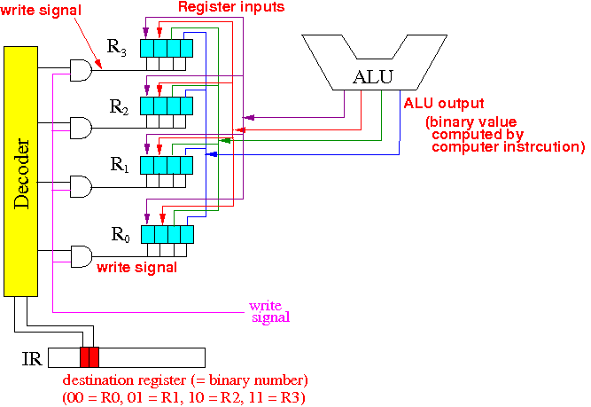
Recall how the ALU output is connected to the registers as follow:

- Each register consists of 4 D-latches.
- The input of a D-latch is connected to some output of the ALU (so that the D-latch can remember the output bit)
- The write signal of the D-latch is connected to a write signal that the CPU uses to write a register. The CPU must generate a write signal only after the ALU has computed the result (that should be obvious, otherwise, you would record the wrong result....)
- The write signal is filtered by a set of and gates controlled by a decoder, so that only the selected register (selected by the decoder) will receive the write signal and gets updated. All the other (unselected) registers will not get the write signal and they will "remember their old value".
- The destination field in the computer instruction is used to select the register for writing - see the connection from the destination field of the IR (instruction register) to the control inputs of the decoder...
/home/cs355001/bin/cs355sim /home/cs355001/demo/circuits/alu-reg |
How to work with this circuit:
- Use keys 0, 1, 2, 3 to set a value which represents the outputs of the ALU
- Use keys a, b to select a register to write the value to. You can see in the probes next to the decoder which register is selected.
- Use key c to trigger the WRITE signal. You should tap c twice (quickly), because that's how the CPU write registers: by turning it on and then off very quickly.
Have fun...