- What you have learned in the last few webpages is what
the distributed system experts call the
"read after write synchronization error"
or "read after write data hazard"
- The "read after write data hazard"
is created by a consumer instruction
(using a register value) that obtained an out of data
value written by a producer instruction (using the same
register as target).
- We saw one type of instruction that produces value for registers:
ALU instructions that update a register
- Recall there are 3 types of instruction: ALU, Memory access (LDR, STR)
and Branching
- Branch instructions do not update registers, so they cannot
cause any read after write data hazards.
- The STORE instruction does not update registers, so neither can
a STORE instruction cause read after write data hazard
- However.... the LOAD instruction does update registers.... oh boy.... here we go again...
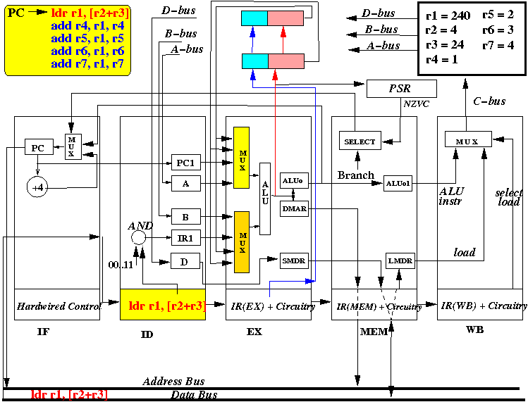
- Consider the following program that is executed by the basic pipeline:
   ldr r1, [r2+r3]      // R1=240, R2=4, R3=24, R4=1, R5=2, R6=3, R7=4
			// Value in  R1 = 240 = 00001111 00000000 (bin)
			// Suppose Memory[28] = 11111111 00000000 (bin)

   add r4, r1, r4       // Correct R4 = 11111111 00000001
   add r5, r1, r5       // Correct R5 = 11111111 00000010
   add r6, r1, r6       // Correct R4 = 11111111 00000011
   add r7, r1, r7       // Correct R4 = 11111111 00000100
   ...
- The correct behavior is:
- The instructions the follows "ldr r1, [r2+r3]" must use the value from memory (= 11111111 00000000 (bin))
As you will see later:
- This is not the case
even using the
forwarding register
improvement !!!
Some instructions will use the old value (= 240) in register R1
Slideshow:
 (Cycle 1: fetch the LDR instruction in ID stage)
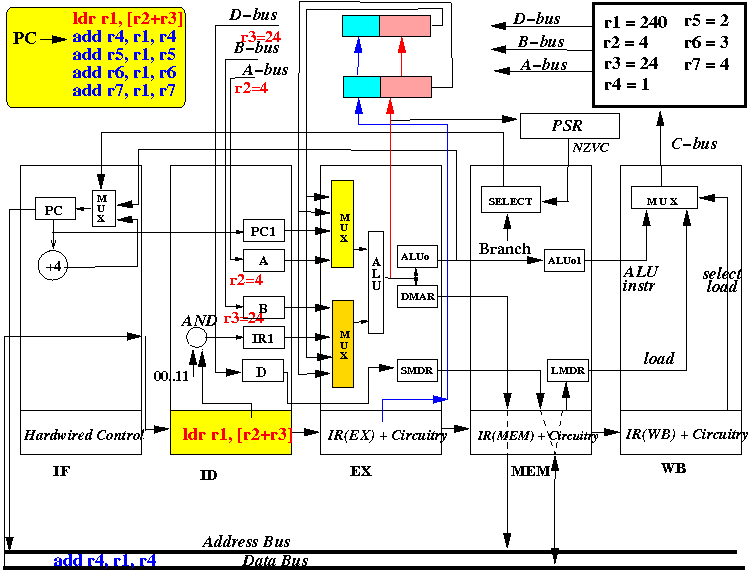 (Start of cycle 2: ID stage fetch operands)
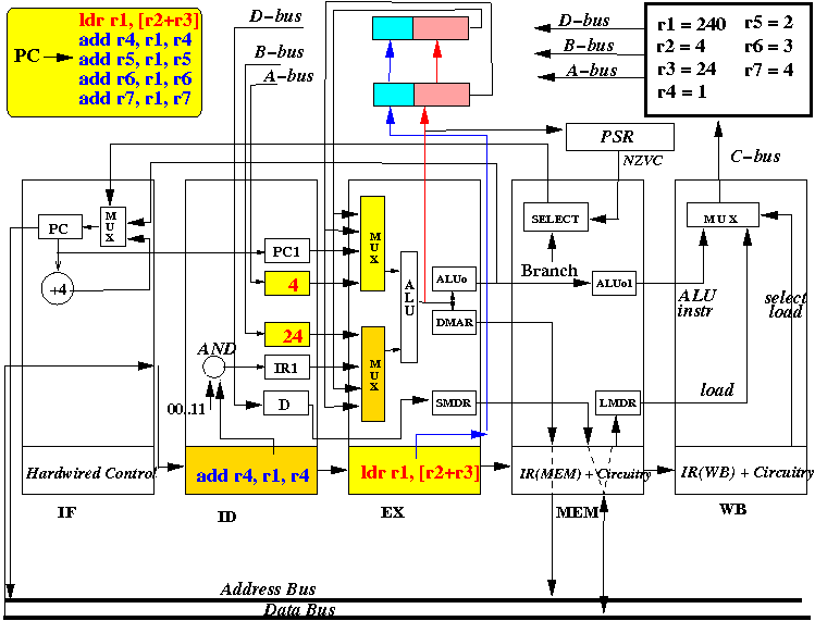 (End of cycle 2: operand fetched, LDR instruction advances, "add" instruction fetched)
 (Start of cycle 3: EX stage computes on operands, ID stage fetches (wrong r1) operands )
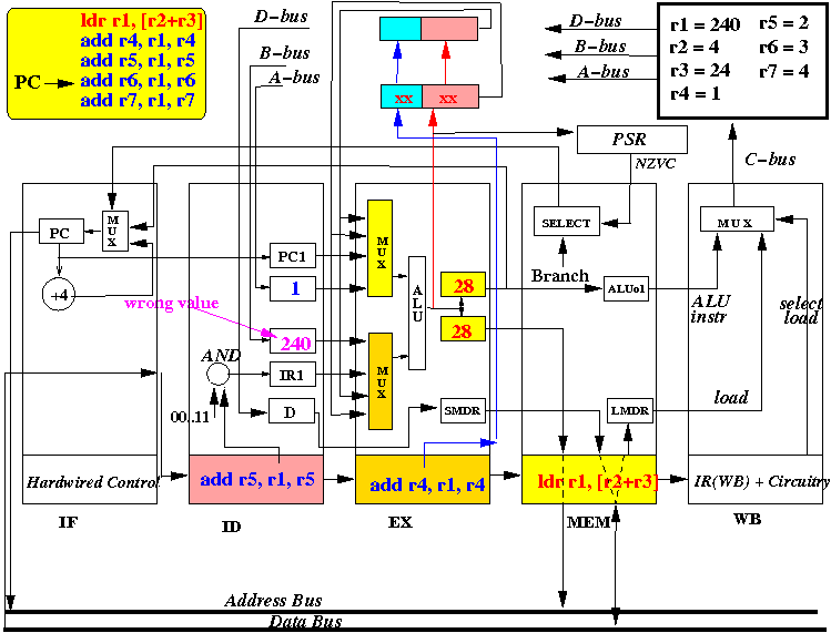 (End of cycle 3: EX resulted memory address in DMAR register, ID stage fetched wrong r1, all instructions advance)
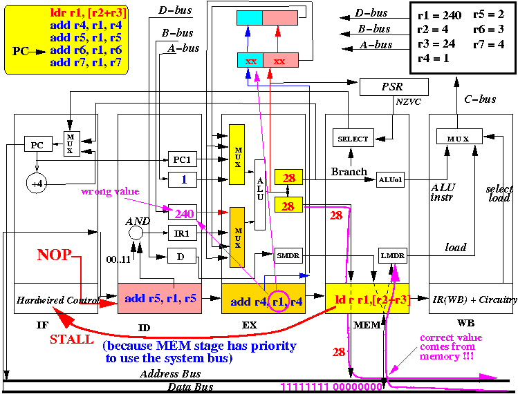 (Start of cylce 4: MEM stage execute LDR instruction --- read memory location 28, EX stage operates on (wrong) r1, ID stage fetches operands, IF stage STALLS )❮ ❯
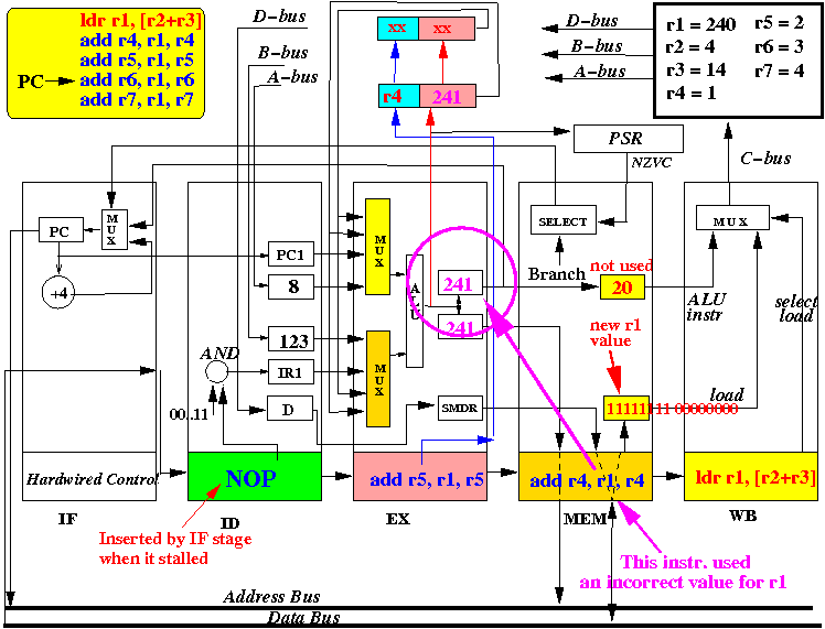 (End of cycle 4: MEM stage did nothing, instruction advances
- At start of the CPU cycle, the IF stage sends out PC
- At end of the CPU cycle, the IR(ID) register is updated with
the instruction fetched (ldr r1, [r2+r3])
State of the CPU at the end of cycle 1:
- The picture above depicts the content of the CPU at end of the first CPU cycle (and the start of the 2nd cycle)
- At start of the CPU cycle, the ID stage sends out selection
signal that selects values from R2 and R3
- At end of the CPU cycle, "A" register is updated with R2 = 4, "B" register is updated with R3= 24.
- Also, at the end of the CPU cycle, the instruction (ldr r1, [r2+r3]) is
moved into IR(EX) and instruction ADD R4, R1, R4 is fetched
into IR(ID)
State of the CPU at the end of cycle 2:
- The picture above depicts the content of the CPU at end of the second CPU cycle (and the start of the 3rd cycle)
- At start of the CPU cycle, the EX stage selects
values from R2 and R3 for the ALU, use the ALU opcode
to make ALU add the input values
4 + 24 forming the
address 28
for the LOAD instruction:
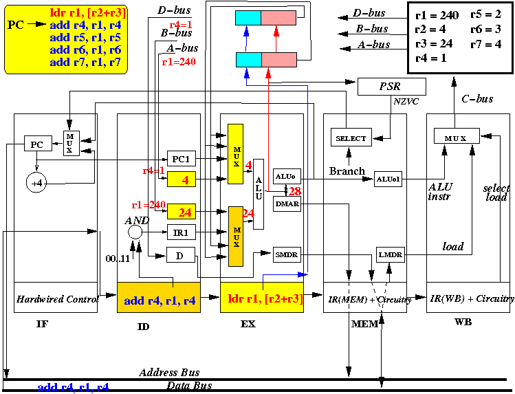
Notice that 28 is an address (in the memory), and the value must still be fetched from this memory location and then stored in register R1
Also, at start of the CPU cycle, the ID stage selects registers R4 and R1 to be fetched into the "A" and "B" registers.
- Register R1 has an old (= incorrect) value at this moment !!!
- At end of the CPU cycle, ALUo and DMAR registers is updated with
the value R1+R2 = 20 (future value of R1)
The LOAD instruction does NOT produce a valid result for the destination register. So we enter an INVALID tag into the Tag Register of Forwarding Register 1 to prevent the value being fetched by the multiplexor.
An invalid tag is easy to formulate: suppose you have 8 registers in the CPU, just enter the value 9 or higher into the tag register or we can add one more bit in the tag register field to indicate if the tag is "valid".
Also, at the end of the CPU cycle, A is updated to R4 (=1) and B is updated to the "current value" of R1 (= 123). This "current" value is a wrong value because there is a more current one on the way from the memory....
Notice that the CPU - at this moment - does not have a clue what that "more current value of R1" is.... because the CPU must still get that value from the memory....
Also, at the end of the CPU cycle, the instruction (ldr r1, [r2+r3]) is moved into IR(MEM), ADD R4, R1, R4 is moved into IR(EX) and instruction ADD R5, R1, R5 is fetched into IR(ID)
- The picture above depicts the content of the CPU at end of the 3rd
CPU cycle (and the start of the 4th cycle)
- Intermezzo:
- Notice the difference in an
ALU hazard instruction
(that we saw previously):

Difference between the load instruction and the add r2,r3,r1 instruction:
- The result of the
add r2,r3,r1 is
now available
in the data forwarding register !!!
- The "result" of the ld [r2+r3],r1 is not available (is coming from the memory !!!)
- The result of the
add r2,r3,r1 is
now available
in the data forwarding register !!!
- We can conclude that the following instruction
ADD R4,R1,R4
will not execute correctly
with any forwarding solution
....
Because:
- In order to forward the data,
you must have the date
available inside the CPU
- At this moment in the execution,
the result is being brought to
the CPU...
- If you have nothing to forward, there is no forwarding solution possible !!!
This kind of data hazard is more severe than the ALU instruction kind...
It necessitate slowing down the pipeline - we will see the solution later...
- In order to forward the data,
you must have the date
available inside the CPU
- Notice the difference in an
ALU hazard instruction
(that we saw previously):
- LD stage:
At start of the CPU cycle, the address in LMAR (= 20) is sent
on the address bus and the value in the memory location 20 is
being fetched. This value will arrive
towards the end of the CPU cycle (because the memory
is pretty slow).
- EX stage:
Also at start of the CPU cycle, the
EX stage
obtain
values from R4 and the
old value
of R1 for the ALU,
because
- The
forwarding registers
does not
have the
new value of
R1
(The value is still being fetched from memory !!!)
- The
forwarding registers
does not
have the
new value of
R1
- ID stage:
Also, at start of the CPU cycle, the
instruction
add r5,r1,r5 in the
ID stage selects
R1 and an
stale value of R1
will be
fetched into the
B register.
- IF stage: Notice that the LOAD instruction in MEM stage will cause the IF stage to STALL
The following figure summarizes the situation before the instructions are executed:
|
|
- At the
end of the
CPU cycle:
- MEM stage:
the LMDR register in MEM stage is updated with
the value fetched from memory (4000).
- EX stage: the instruction
ADD R4,R1,R4 has updated ALUo (and DMAR) registers with
the value INCORRECT value R4+R1 = 124
(R1 should be equal to 4000).
- ID stage: A is updated to R5 and
B is updated to the old value of R1
.
- IF stage:
feeds a
NOP instruction
into the ID stage
- Instructions are
moved forward:
- the instruction (ldr r1, [r2+r3]) is moved into IR(WB),
- ADD R4, R1, R4 is moved into IR(MEM),
- instruction ADD R5, R1, R5 is moved into IR(EX) and
- the instruction NOP is inserted into IR(ID) (See: click here )
- MEM stage:
the LMDR register in MEM stage is updated with
the value fetched from memory (4000).
|
|
- The picture above depicts the content of the CPU at end of the 4th
CPU cycle (and the start of the 4th cycle)
- add r4,r1, r4 has used an incorrect value for r1 !!!
- We can see that R4 will be updated with an
incorrect value
by the
pipelined CPU.