Review:
interconnecting CPU and the memory
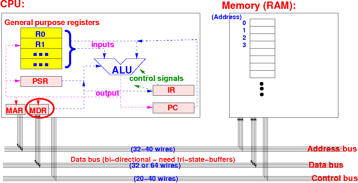
In CS255, you learned how the CPU and memory is connected in this way:
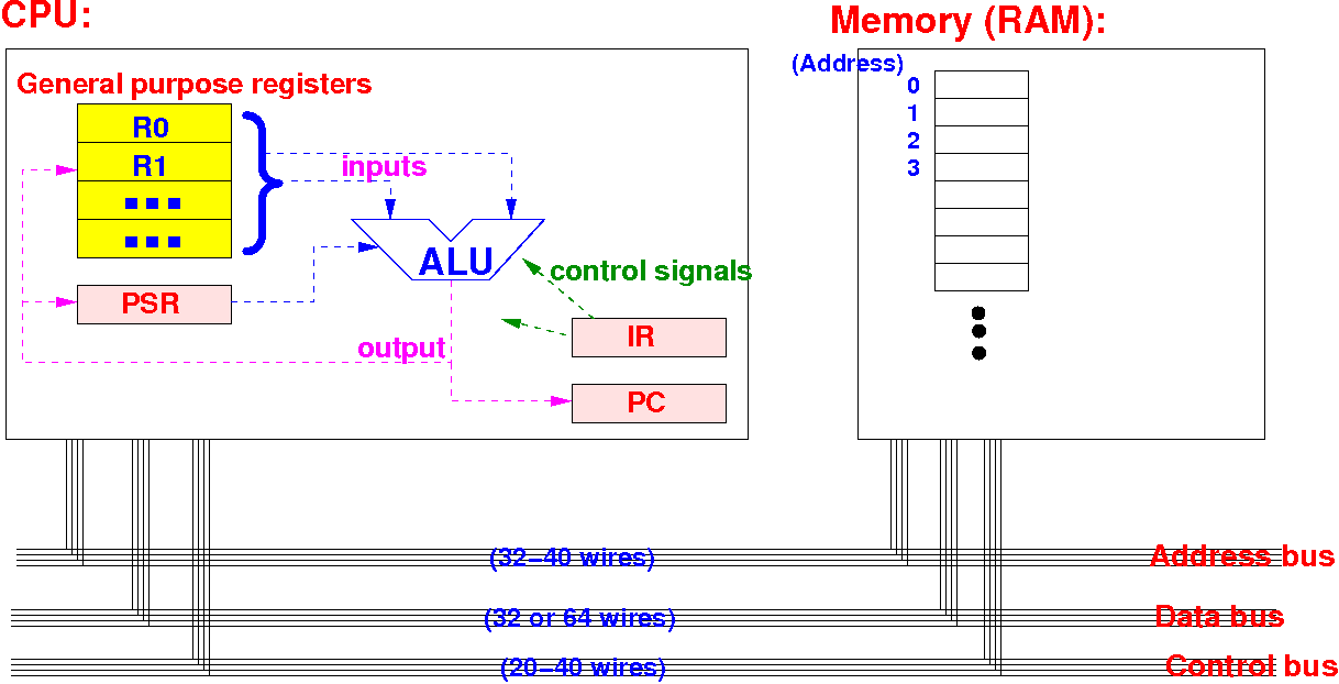
CS255 has omitted some special purpose registers for simplicity !!
These special purpose registers are "buffers" used to store intermediate data to simplify the circuitry
Special register #1:
MAR
--
used to send addresses onto the address bus
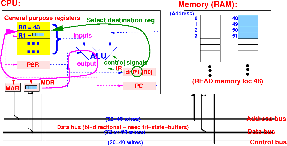
The Memory Address Register (MAR) contains the address value sent on the address bus:
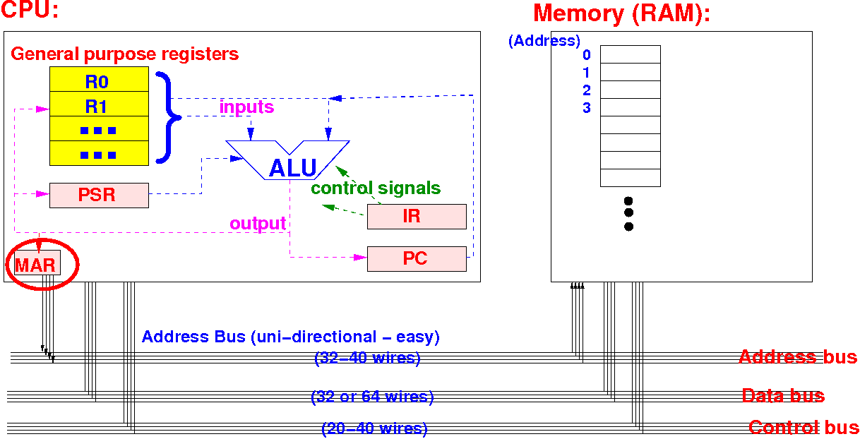
The MAR contains an address
The MAR's purpose is to transmit the address on the address bus (it must keep the address signals stable)
Special register #1:
MAR
--
used to send addresses onto the address bus
Example: when CPU executes ldr R1,[R0], the CPU first writes R0 into the MAR register:
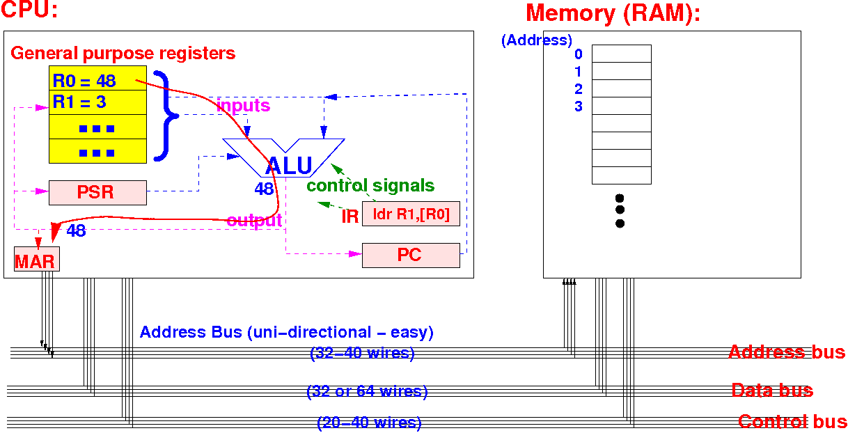
Special register #1:
MAR
--
used to send addresses onto the address bus
Example: ... and then the MAR register sends its address onto the data bus (wires):
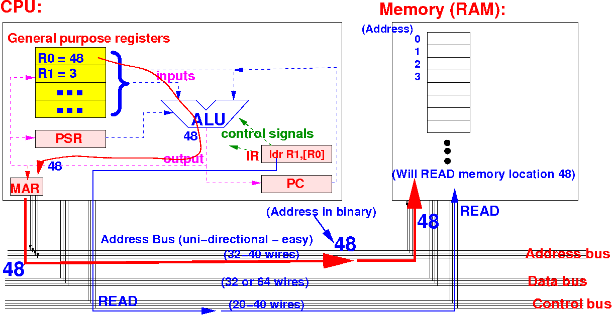
How to
connect the
MAR register
to the address bus
The MAR register consists of N (32 to 35 or so) D-flipflops (depends of memory size):
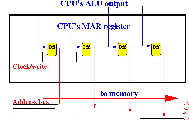
The inputs of the
D-flipflops are
connected to the
ALU output
The outputs of the
D-flipflops are
connected to the
address bus
The (uni-directional) address bus will send the address value in the MAR to the memory (circuit).
Special register #2:
MDR
--
used to send/receive data on the data bus
The Memory Data Register (MDR) is used to buffer the data being send/receive on the data bus:
The MDR contains the data in transit (being transfered) between the CPU and the memory
Special register #2:
MDR
--
used to send/receive data on the data bus
Example: when CPU executes ldr R1,[R0], the memory will return the data at address R0
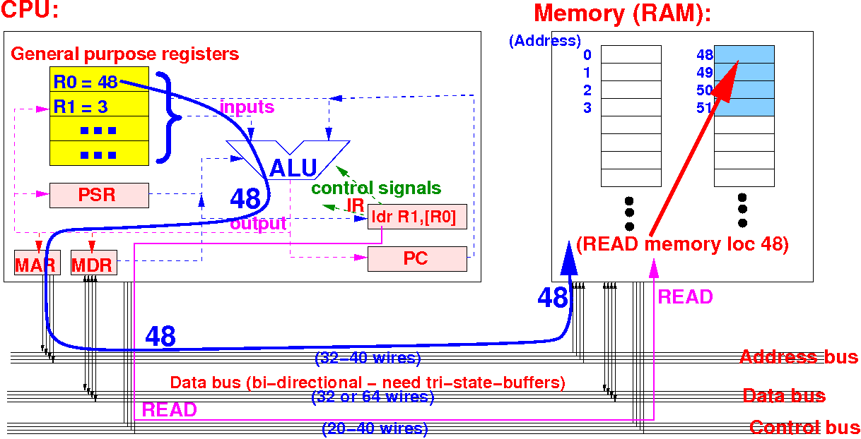
Suppose the databus has 32 bits: then 4 bytes starting at address 48 are transfered
Special register #2:
MDR
--
used to send/receive data on the data bus
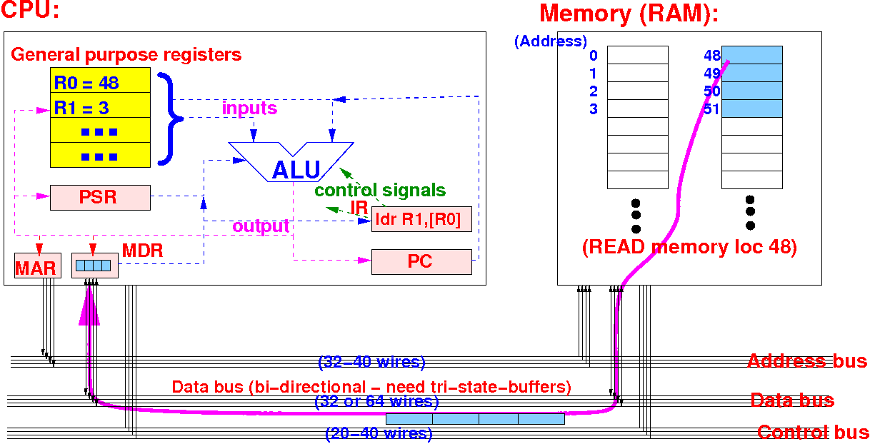
Example: ... the memory data is first stored in the MDR register
Special register #2:
MDR
--
used to send/receive data on the data bus
Example: ... and then forwarded to the destination register R1
How to
connect the
MDR register
to the data bus
The MDR register consists of N (32 or 64) D-flipflips:
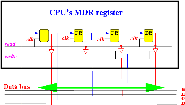
The outputs of the D-flipflops must be connected through tri-state-buffers to prevent short-circuit (because the databus is bi-directional) !!
Next topic:
how to connect a memory circuit
to the
system bus
Next, we will study how to connect a memory circuit to the system bus:
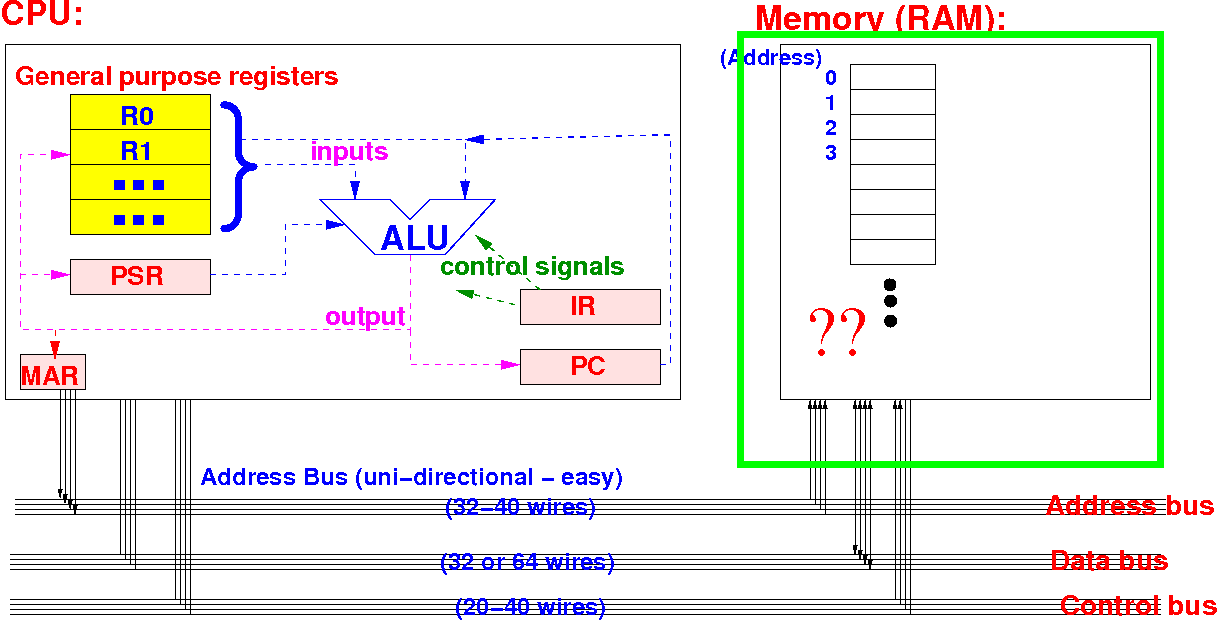
Important fact: the memory circuit must handle both read and write operations !!
Background info:
the CPU's actions in a
read operation to the
memory
The CPU sends
(1) the
address on the
address bus and
(2) a
READ command on the
control bus:
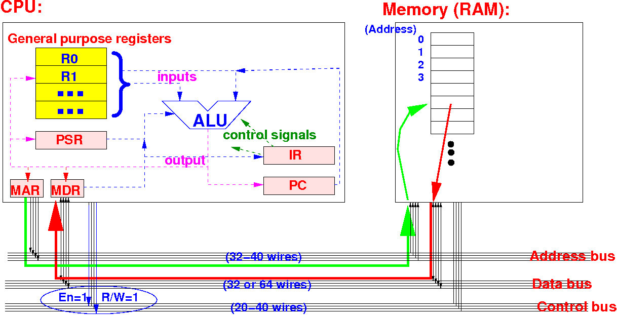
The READ command is expressed using the signals: EN (enable)=1 and R/W (Read/Write)=1
Note: In response, the memory sends back the requested data
Background info:
the CPU's actions in a
write operation
to the memory
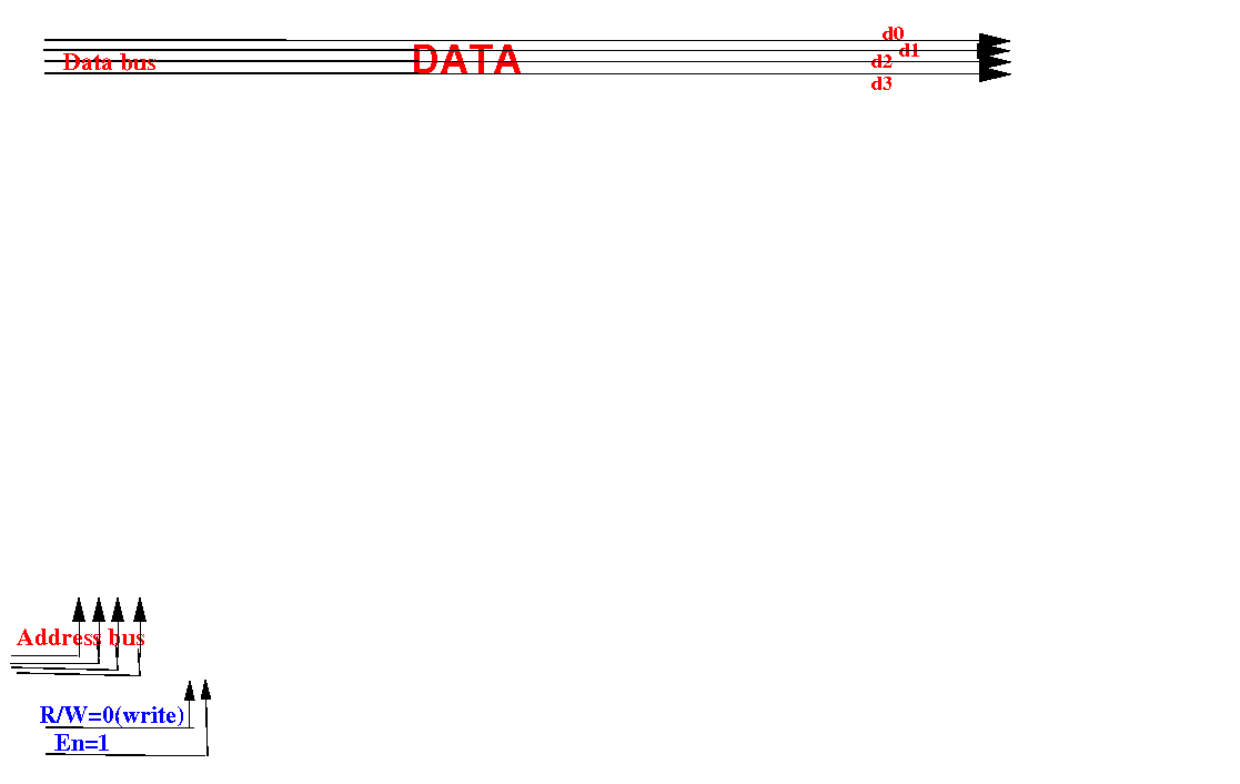
The CPU sends (1) the address on the address bus, (2) the data on the data bus and (3) a WRITE command on the control bus:
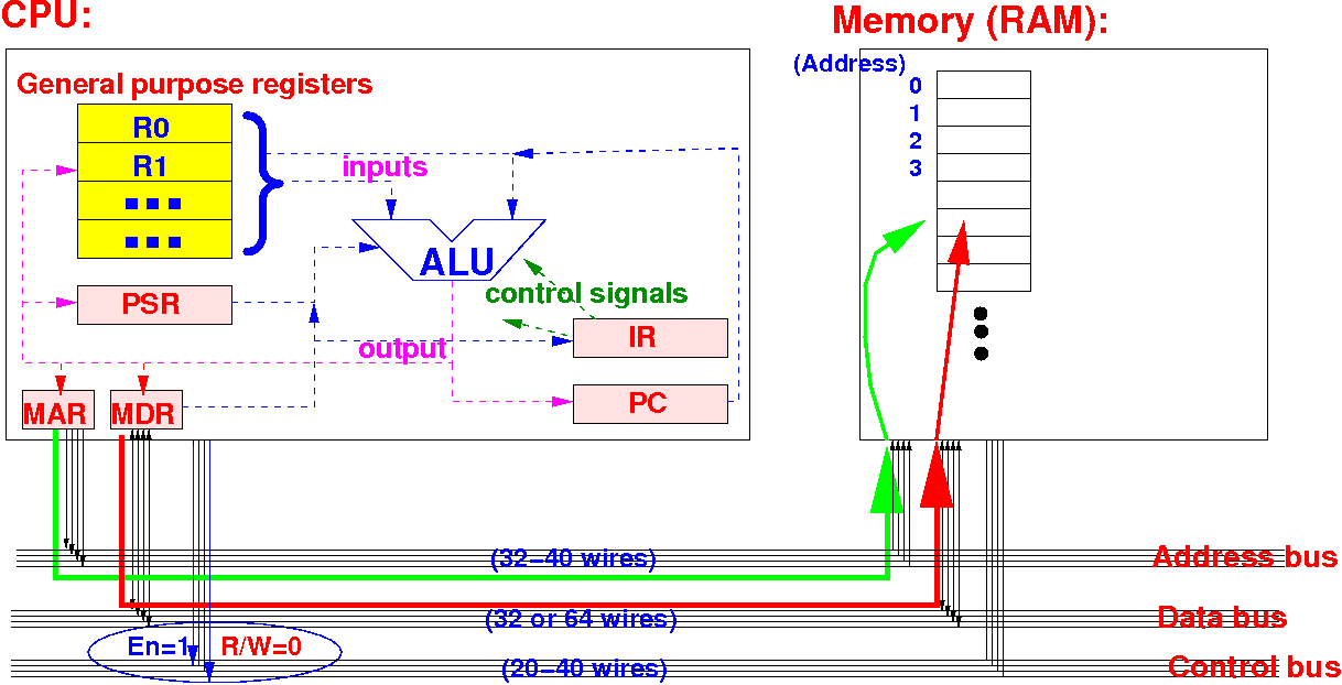
The WRITE command is expressed using the signals: EN (enable)=1 and R/W (Read/Write)= 0
Note: In response, the memory stores the sent data
Background info:
the effect of the
width of the databus
on the computer memory
|
The effect of the
width of the databus
on the computer memory
Example: in order to read any data from memory 0, 1, 2, 3 , the CPU uses address 0:
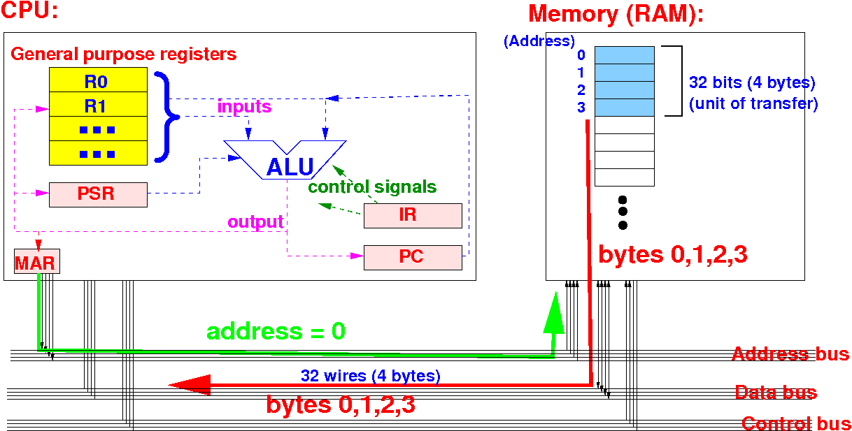
This is the reason why programming languages impose the alignment requirement...
The effect of the
width of the databus
on the computer memory
Example: in order to read any data from memory 4, 5, 6, 7 , the CPU uses address 4 :
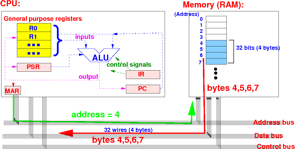
This is the reason why programming languages impose the alignment requirement...
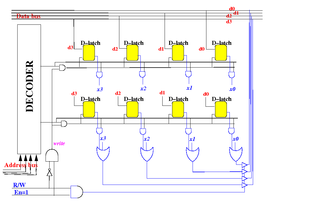
The memory circuit
(how to connect a memory circuit)
For now, take note of the locations of the address, data and control buses in this diagram:
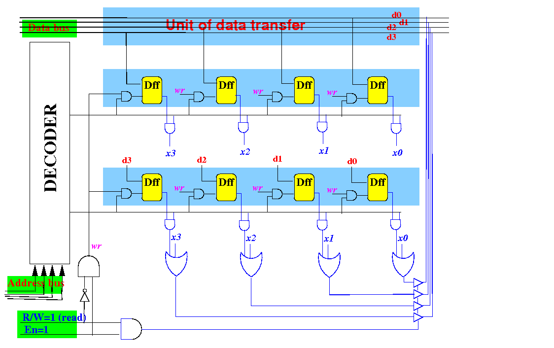
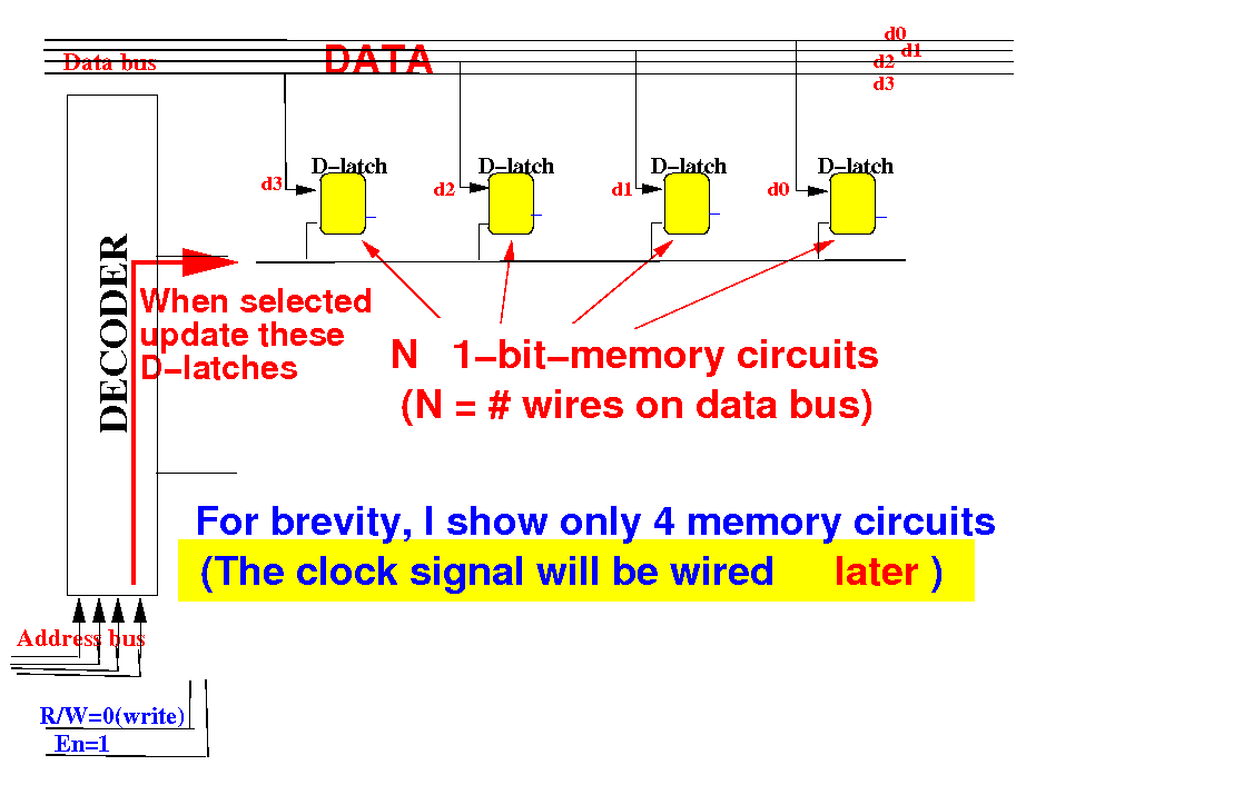
Each row of the memory circuit contains the same number of Dffs as the number of wires on the data bus (= unit of transfer)
Connecting a memory circuit to
execute the
write operation
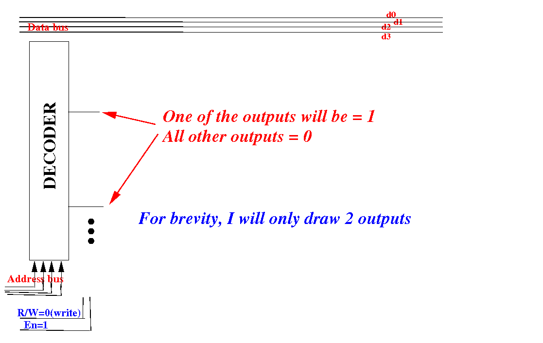
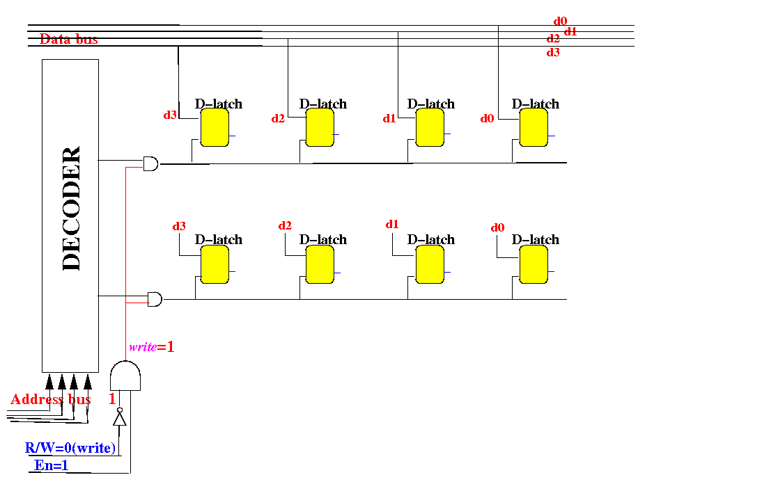
The CPU sends out the address, the data and a write command on the system bus:
Connecting a memory circuit to
execute the write operation
We use a decoder to translate the address into a selection:
Connecting a memory circuit to
execute the write operation
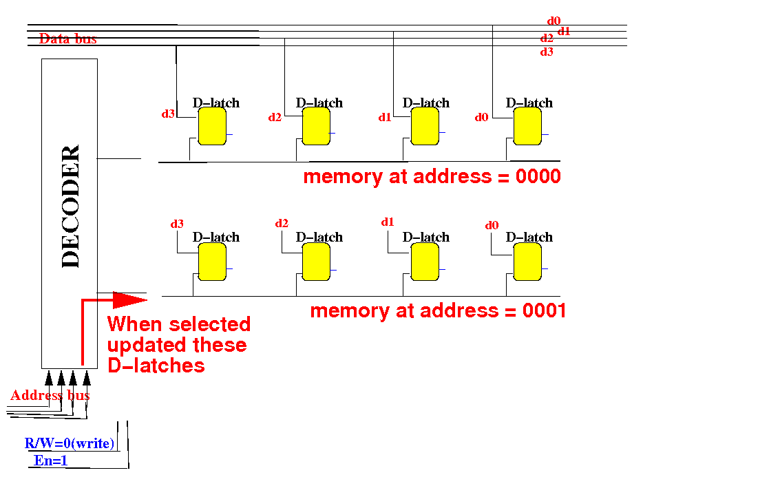
Connect N 1-bit-memory to receive the data for address=0000
Connecting a memory circuit to
execute the write operation
Connect another N 1-bit-memory to receive the data for address=0001
Connecting a memory circuit to
execute the
write operation
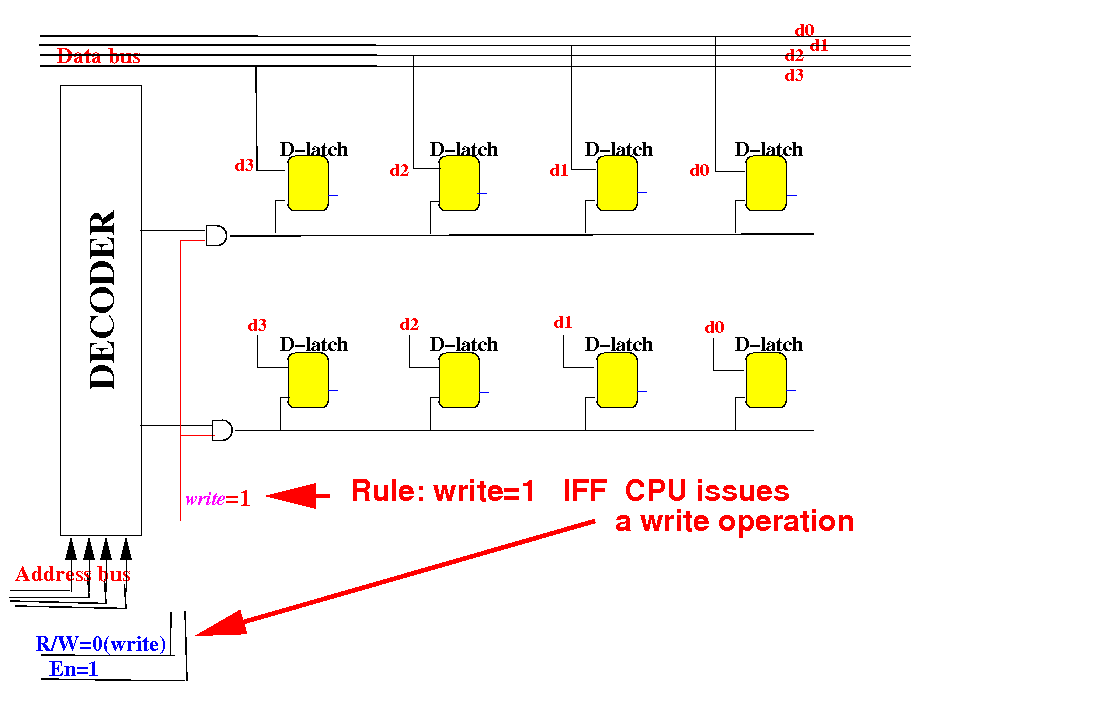
We control to writing of a row of memory cells by a write signal:
Connecting a memory circuit to
execute the
write operation
Make the (simple) write control circuit:
Connecting a memory circuit to
execute the
write operation
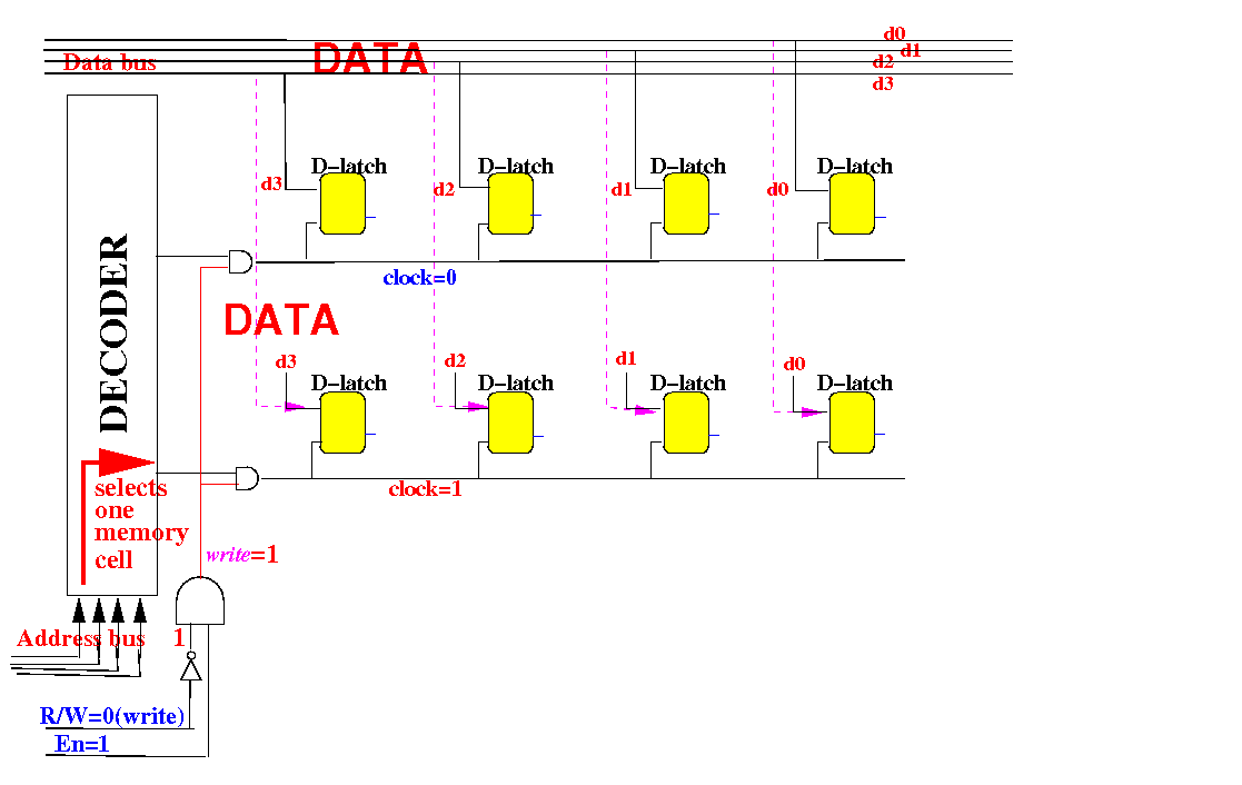
Sample operation: if memory cell 0001 is selected, the data is stored in the 1st row of cells
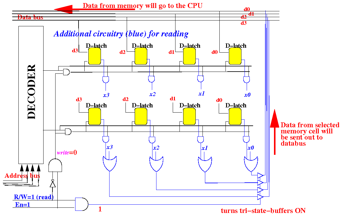
Connecting a memory circuit to
execute the
read operation
Consider the memory circuit we have so far: (connected for the write operation)
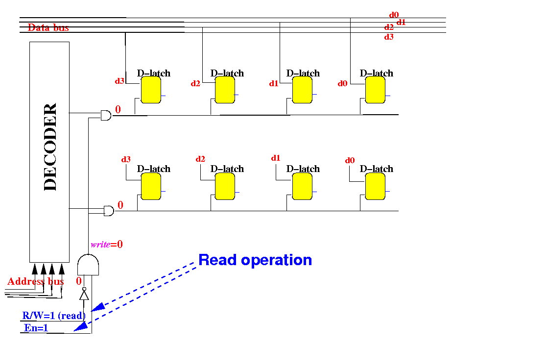
What will the memory circuit do if the CPU sends out a READ command/operation ???
Connecting a memory circuit to
execute the
read operation
Notice that the circuit will not update any of the memory cells: (which is the correct behavior !)
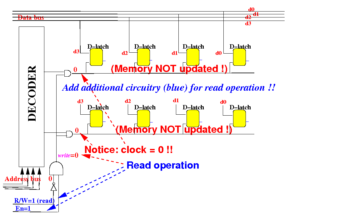
The AND gate will output 0 which prevents the Decoder outputs from writing any memory cell
Connecting a memory circuit to
execute the
read operation
We use a decoder output as a filter control signal on the outputs of a row of memory cells:
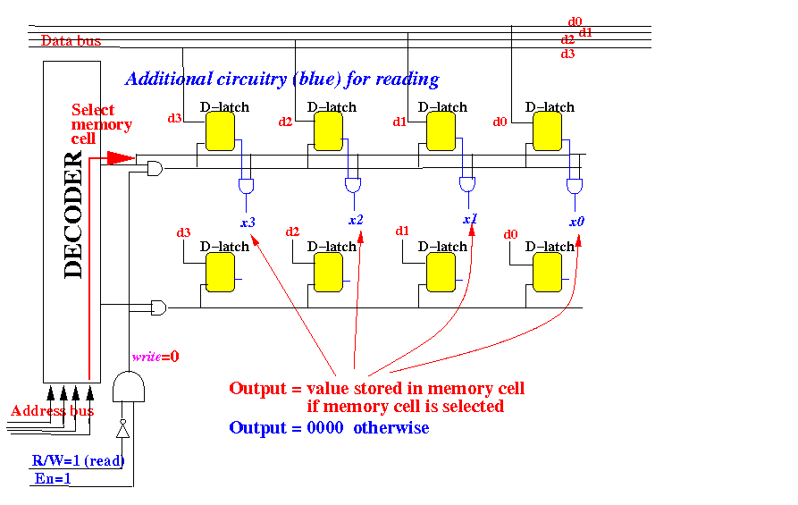
The filtering is necessary because we will (later) use an OR gate to collate all the bits
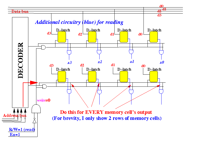
Connecting a memory circuit to
execute the
read operation
Repeat the filtering connection for every row of memory cells:
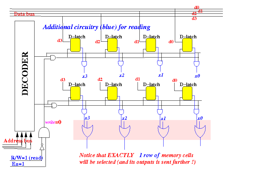
Connecting a memory circuit to
execute the
read operation
Use an OR-gate to collate all the outputs (all but 1 row will be non-ZERO !):
Connecting a memory circuit to
execute the
read operation
Connect the outputs to the data bus through tri-state-buffers:
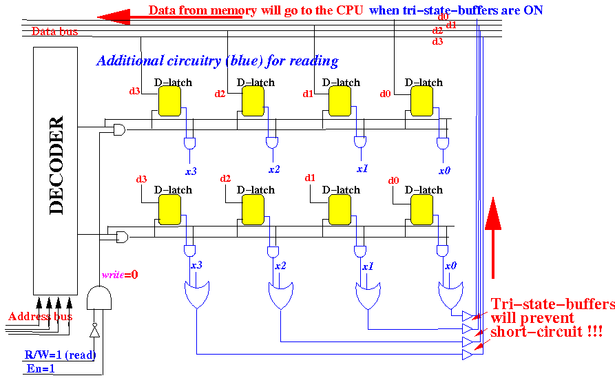
Connecting a memory circuit to
execute the
read operation
We activate the tri-state-buffers when the CPU issues a READ operation:
Demo the memory circuit
DEMO: /home/cs355001/demo/circuits/memory-circuit
Comment:
the reality is more complicated
|
Communication protocols
|
Postscript: static and dynamic memory
|