Background information
|
Background information
|
Background information
|
Background information
|
DEMO: /home/cs355001/demo/circuits/shift-register
A simple experiment using
D-latches
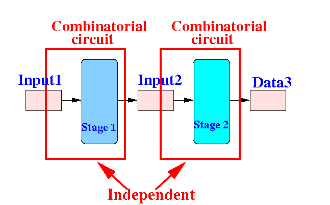
The following simple circuit shows a problem with D-latches when we try to build a independent staged computation device with them:
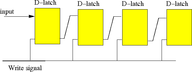
In this circuit, each of the D-latch (= 1-bit-memory circuit) will copy the bit stored in the prior 1-bit-memory circuit into itself.
DEMO the behavior: /home/cs355001/demo/circuits/shift-reg-D-latch
A simple experiment
using D-latches
|
We will first study circuit timing and then build a accurate 1-bit-memory circuit
Background information
|
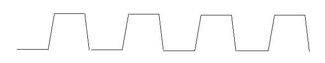
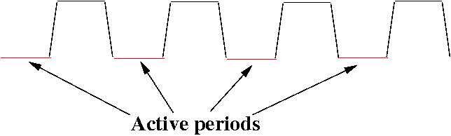
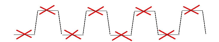
Active period of a memory circuit
|
Active periods for the
D-latch circuit

|
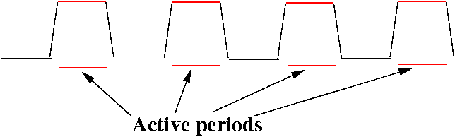
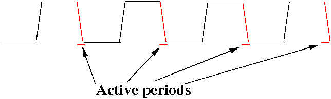
Inactive periods for the
D-latch circuit
|
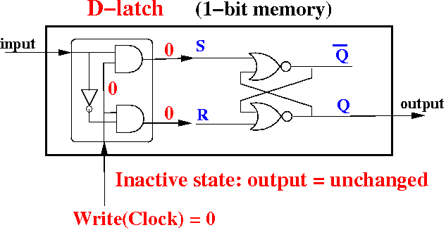
Latches: level active (level triggered) memory devices
|
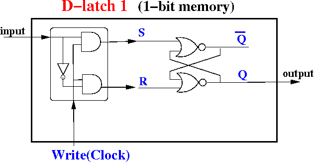
Latches: level active (level triggered) memory devices
|
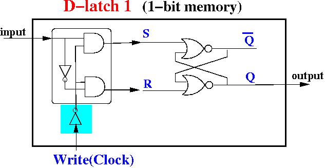
Latches: level active (level triggered) memory devices
|
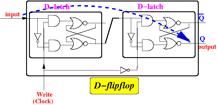
The D-flip flop circuit
Consider the following circuit (it's called a D-flip flop):
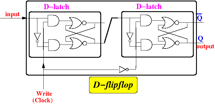
What are the active periods of this circuit ?
Use the DEMO to find out: /home/cs355001/demo/circuits/d-flipflop-demo
The D-flip flop circuit
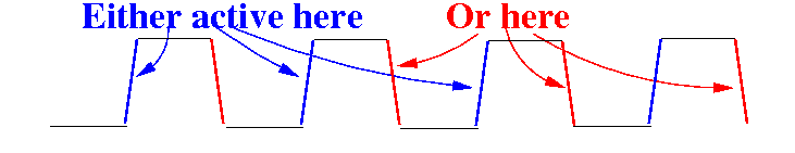
Let's eliminate the non-active periods:
The D-flip flop is not active during clock level = 0:
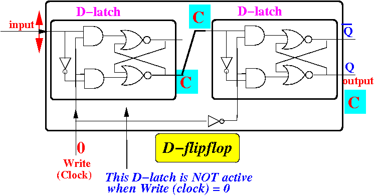
The D-flip flop circuit
Let's eliminate the non-active periods:
The D-flip flop is not active during clock level = 1:
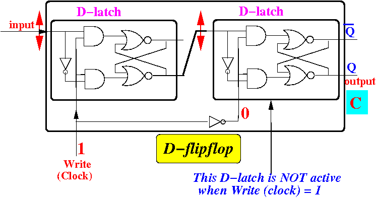
The D-flip flop circuit
Notice that we can (= are able to) update the output = input (see demo):
So the D-flip flop must have an active period that is edged:
Flip flops: edge active (edge triggered) memory devices
|

DEMO: /home/cs355001/demo/circuits/shift-register
Accurate and inaccurate memory circuits
|
Fast and slow memory analogy: shutter speed of
a camera
In photography, using a faster shutter speed will capture a more accurate scene/state:
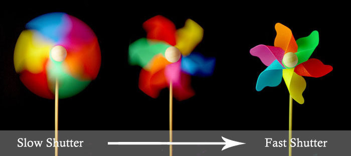
Because a shorter exposure time does not allow much motion...
Introducing EDiSim's
built-in D-flipflop component
|
Introducing EDiSim's
built-in D-flipflop component -
Examples
The D-flipflop components will initially have an UNKNOWN value for output:
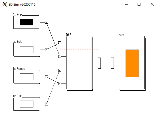
The ORANGE color in the
probe means:
UNKNOWN value
DEMO:
/home/cs355001/demo/circuits/sample-Dff
Introducing EDiSim's
built-in D-flipflop component -
Examples
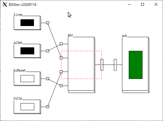
You can initial the output = 0 with reset=1 (and set=0):

The LIGHT GREEN color in the
probe means:
value=0
Introducing EDiSim's
built-in D-flipflop component -
Examples
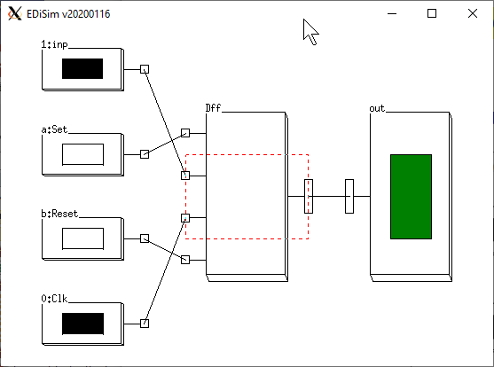
You can initial the output = 1 with set=1 (and reset=0):
The DARKER GREEN color in the
probe means:
value=1
Introducing EDiSim's
built-in D-flipflop component -
Examples
When set=0 and reset=0, the Dff component will operate as a D-flipflip:
The input value will be
written to the
output using the
clock signal