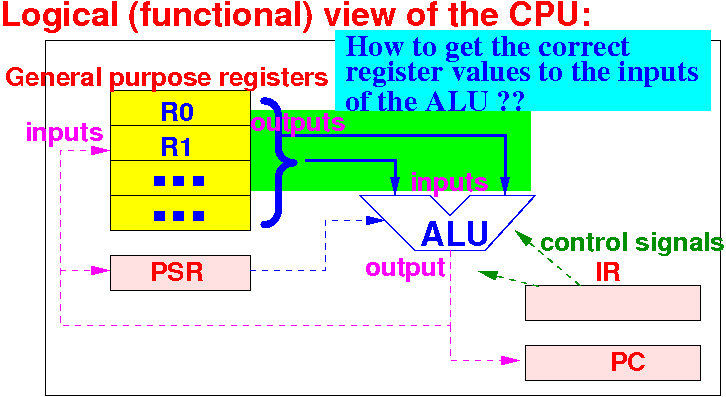
Background review and context of the problem
that we are discussing
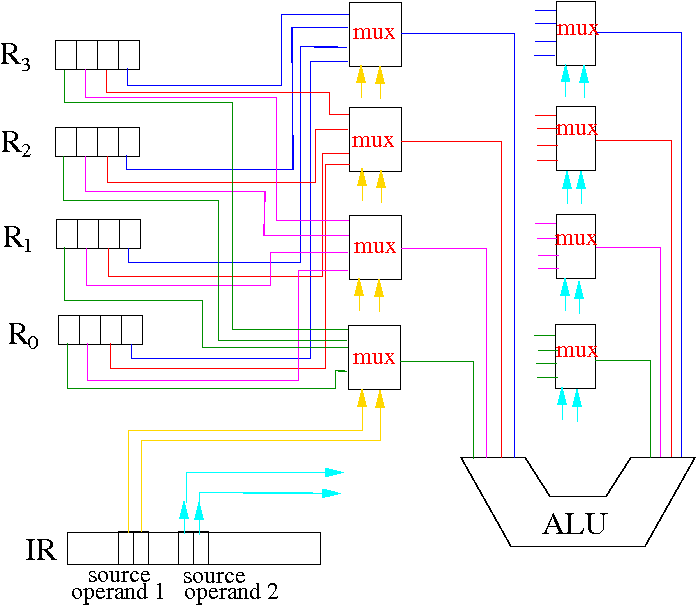
Previously, we studied a circuit that switch the registers' value (= outputs) to the inputs of the ALU:
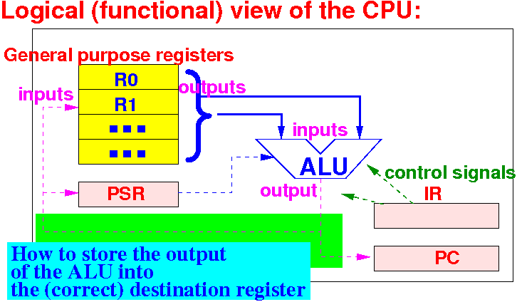
Background review and context of the problem
that we are discussing
In this set of slides, we will study a circuit that stores the ALU output into the correct destination register:
Introduction
|
Operation of a one-bit memory cell
A one-bit memory cell has 2 inputs (data input and write control) and 1 outputs:
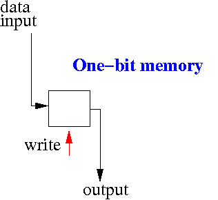
When
write=0, the
output will
remain
unchanged
(= remembers)
When
write=1, the
output become
equal to the
input
(= updated)
DEMO:
/home/cs355001/demo/circuits/1-bit-memory
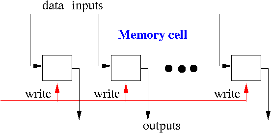
Registers and computer memory cells
A register (or memory cell) consists of N one-bit memories under control by a write signal:
DEMO: /home/cs355001/demo/circuits/4-bit-memory
(The demo shows a
4 bit memory cell, it's
easy to make
an 8 bit or
32 bit memory cell)
Note: we
will study the
internals of
memory cells
later
What we will do next
Now that you have seen how memory cells are written (= updated), I will next:
|
Instruction encoding: how a computer instruction is expressed
Each CPU has its own instruction encoding format.
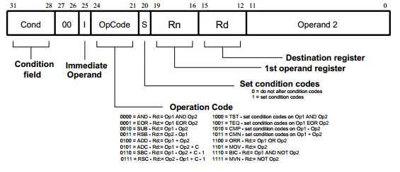
This is the ARM instruction encoding format (each ARM instruction is 32 bits long)
How the CPU uses the different fields
in the ARM instruction
The Rd field is used to select the destination operand for output of the ALU:
Destination register field in the ARM instruction
Sample ARM add assembler instructions:
3 main: 4 0000 081083E0 add r1, r3, r8 5 0004 085083E0 add r5, r3, r8 6 0008 089083E0 add r9, r3, r8 |
Can you spot the place of the destination register number field in the ARM's "add" instruction ???
Destination register field in the instruction
Here they are: (bytes stored in little endian ordering !)
3 main: 4 0000 081083E0 add r1, r3, r8 5 0004 085083E0 add r5, r3, r8 6 0008 089083E0 add r9, r3, r8 |
Can you spot the place of the destination register number field in the ARM's "add" instruction ??? (Did you find the field location ?)
Prelude: we
omit the
selection of registers for the
ALU input
Selecting the (outputs of) registers to the (input of the) ALU has been discussed:
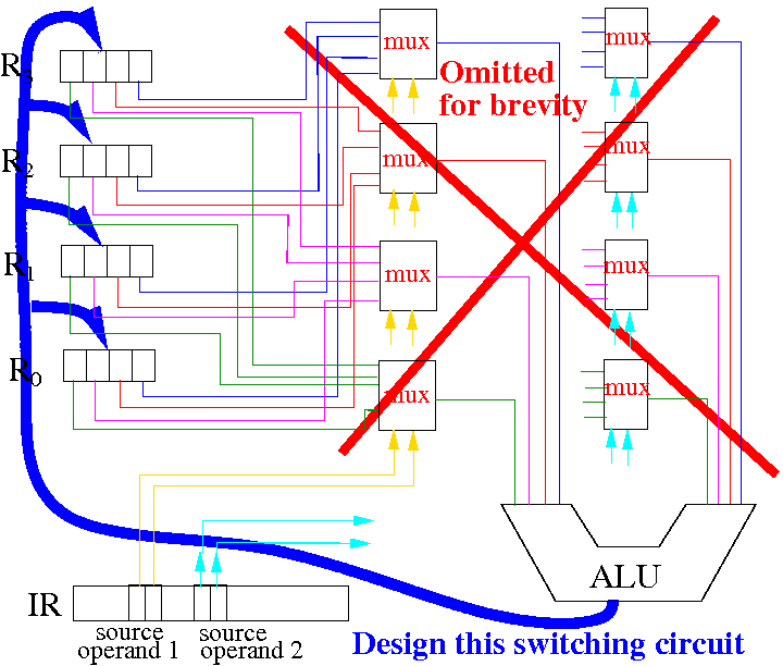
Prelude: we
omit the
selection of registers for the
ALU input
I will only present this switching circuit in the lecture material (for brevity):
How does the CPU use the destination register field
to
select a register
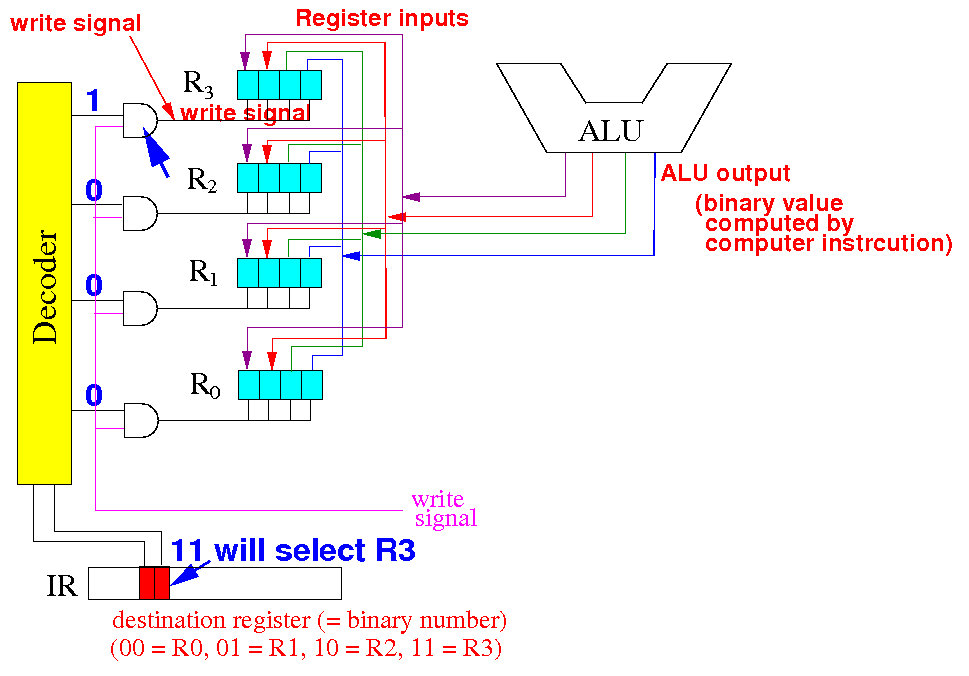
Circuit used to update the destination register with the values (= output) of the ALU:
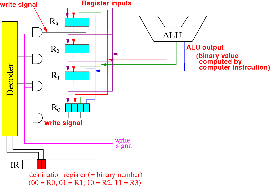
I will explain this circuit in the next few slides...
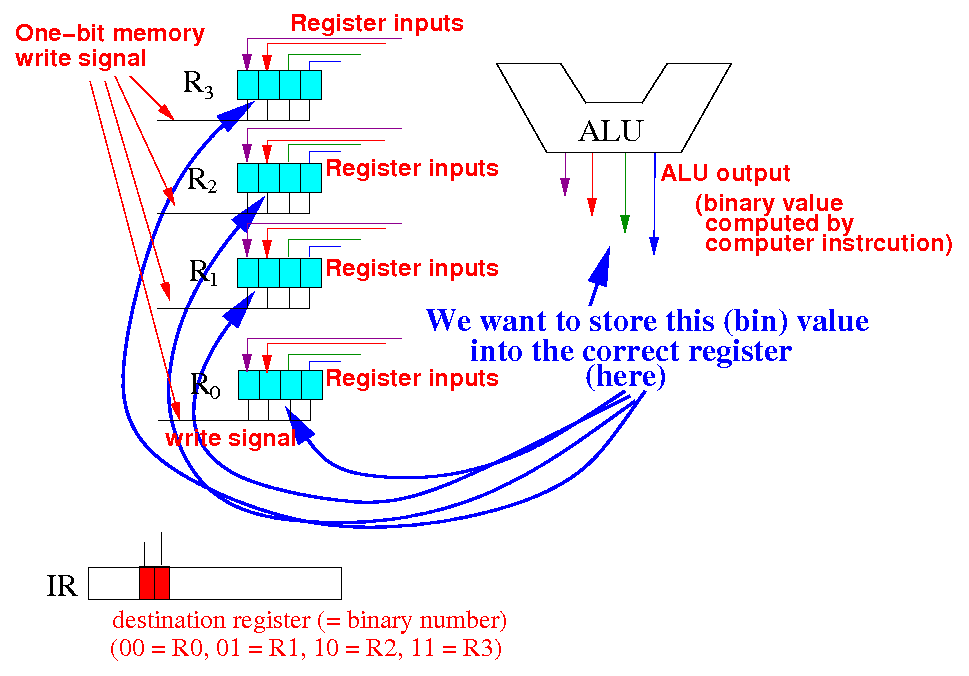
Circuit to
store the
ALU output to
the destination register in
instruction
Problem description:
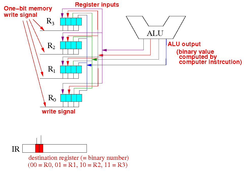
Circuit to
store the
ALU output to
the destination register in
instruction
Connect the output bit of ALU to the corresponding input bit of each register:
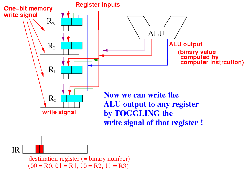
Circuit to
store the
ALU output to
the destination register in
instruction
What have we achieved:
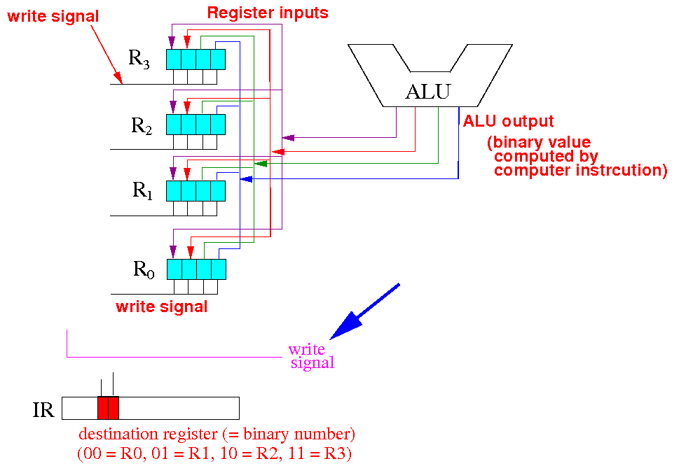
Circuit to
store the
ALU output to
the destination register in
instruction
The CPU has a write signal used to control the time it wants to update registers:
Circuit to
store the
ALU output to
the destination register in
instruction
Use a decoder to select the destination register to write:
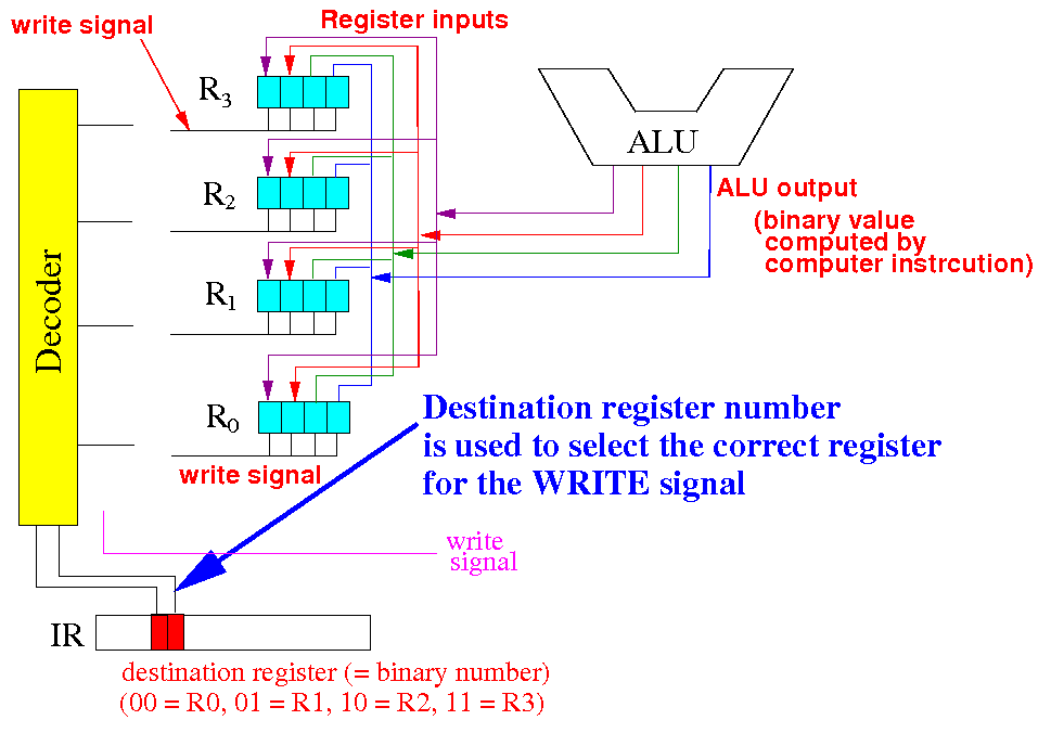
Circuit to
store the
ALU output to
the destination register in
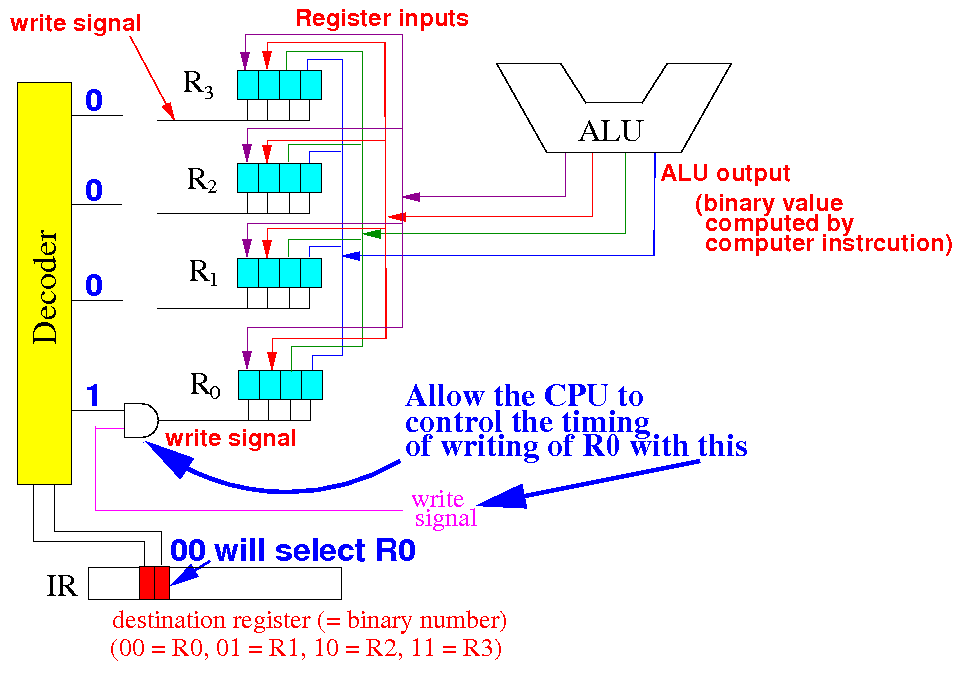
instruction
This AND gate will allow the CPU to control sending a write signal to R0:
Circuit to
store the
ALU output to
the destination register in
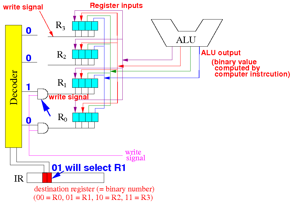
instruction
This AND gate will allow the CPU to control sending a write signal to R1:
Circuit to
store the
ALU output to
the destination register in
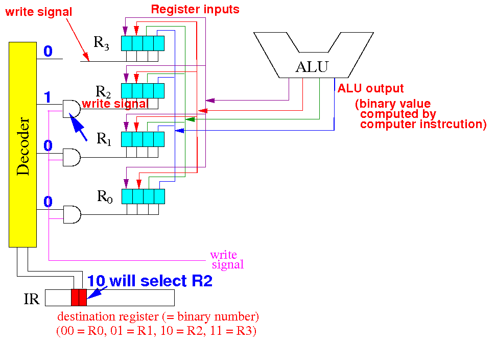
instruction
This AND gate will allow the CPU to control sending a write signal to R2:
Circuit to
store the
ALU output to
the destination register in
instruction
This AND gate will allow the CPU to control sending a write signal to R3:
DEMO
Demo circuit looks like this:
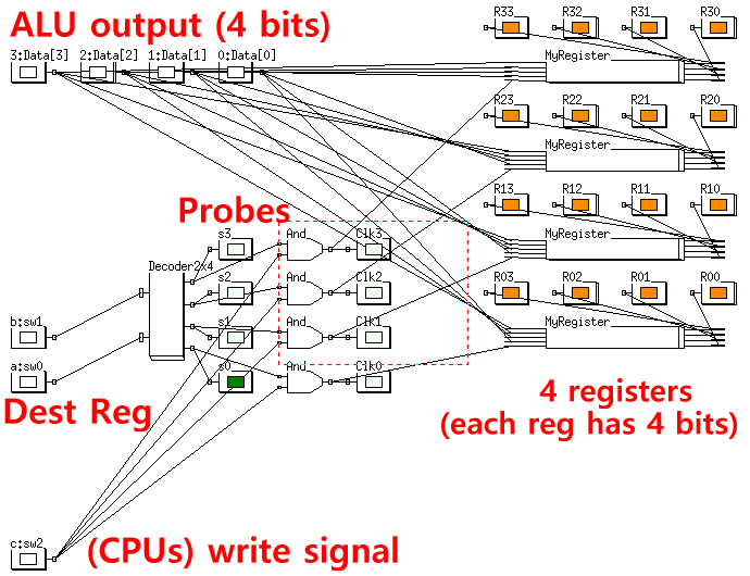
DEMO file: /home/cs355001/demo/circuits/alu-reg