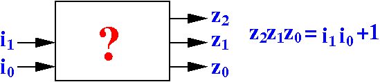
Another circuit design problem
Problem description:
|
(Show the behavior using: /home/cs355001/demo/circuits/add1)
A circuit design algorithm
Step 1: list out every combination of the input values
    i1   i0 | z2   z1   z0
   ----+----+----+----+----
    0    0  |
    0    1  |
    1    0  |
    1    1  |
|
A circuit design algorithm
Step 2: determine the output for each combination of input values
    i1   i0 | z2   z1   z0
   ----+----+----+----+----
    0    0  | 0    0    1    (00 + 1 = 001)
    0    1  |
    1    0  |
    1    1  |
|
A circuit design algorithm
Step 2: determine the output for each combination of input values
    i1   i0 | z2   z1   z0
   ----+----+----+----+----
    0    0  | 0    0    1
    0    1  | 0    1    0    (01 + 1 = 010)
    1    0  |
    1    1  |
|
A circuit design algorithm
Step 2: determine the output for each combination of input values
    i1   i0 | z2   z1   z0
   ----+----+----+----+----
    0    0  | 0    0    1
    0    1  | 0    1    0
    1    0  | 0    1    1    (10 + 1 = 011)
    1    1  |
|
A circuit design algorithm
Step 2: determine the output for each combination of input values
    i1   i0 | z2   z1   z0
   ----+----+----+----+----
    0    0  | 0    0    1
    0    1  | 0    1    0
    1    0  | 0    1    1
    1    1  | 1    0    0    (11 + 1 = 100)
|
A circuit design algorithm
Step 2: determine the output for each combination of input values
|
This is the logic table of the "add 1" function
Note: the logic table actually contains 3 simpler functions (one function for z2, one for z1 and another for z0)
Click on table to pull out
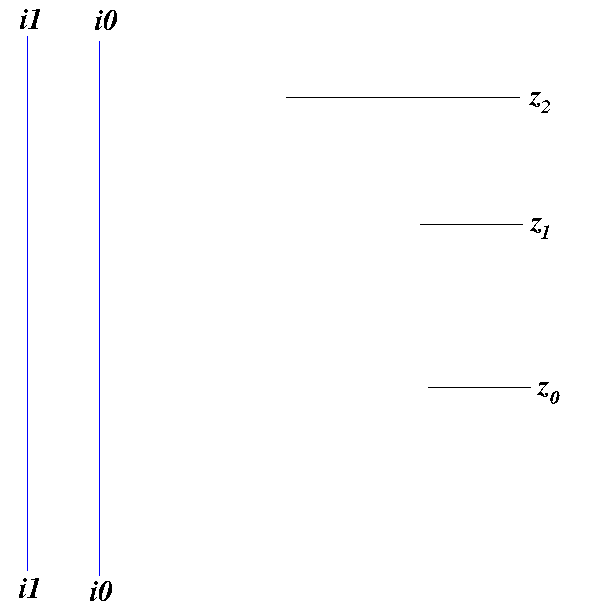
Use the logic table to
construct the digital circuit
Step 1: draw the input signals and the output signal(s)
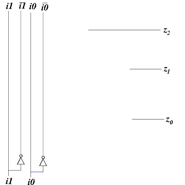
Use the logic table to
construct the digital circuit
Step 2: add the NOT-gates to obtain all possible input combinations:
Use the logic table to
construct the digital circuit
Apply the circuit design technique on output signal z0:
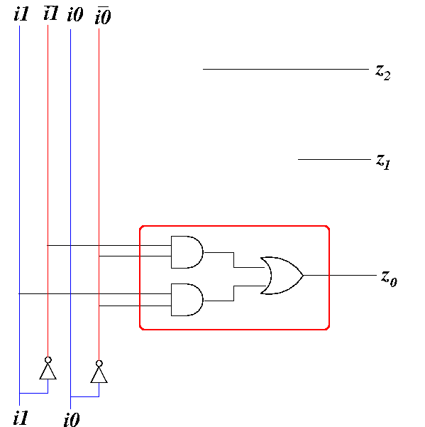
You only use column z0 in the logic table to design this digital circuit!
Use the logic table to
construct the digital circuit
Apply the circuit design technique on output signal z1:
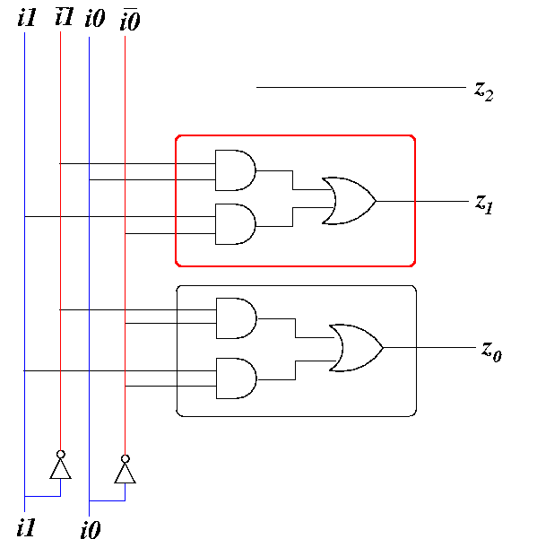
You only use column z1 in the logic table to design this digital circuit!
Use the logic table to
construct the digital circuit
Apply the circuit design technique on output signal z2:
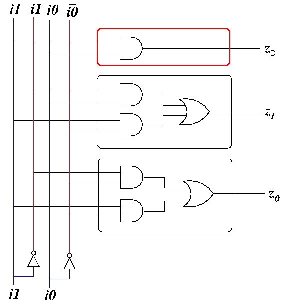
You only use column z2 in the logic table to design this digital circuit!
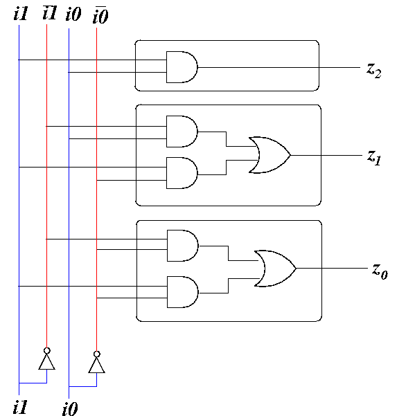
EDiSim circuit simulation program for the "add1" circuit
Switch aa i1 '1' ZERO; Not aa i1 n_i1; Switch ba i0 '0' ZERO; Not ba i0 n_i0; /* ----- z2 ---- */ And ab i1 i0 z2a; Or ac z2a z2; /* ----- z1 ---- */ And bb n_i1 i0 z1a; And bb i1 n_i0 z1b; Or bc z1a z1b z1; /* ----- z0 ---- */ And cb n_i1 n_i0 z0a; And cb i1 n_i0 z0b; Or cc z0a z0b z0; Probe ad z2; Probe bd z1; Probe cd z0; |
(I will write this code interactively in class)
DEMO
I will demo this circuit in class:
Circuit file: /home/cs355001/demo/circuits/add1