The cause of
the read-after-write data hazard
problem
|
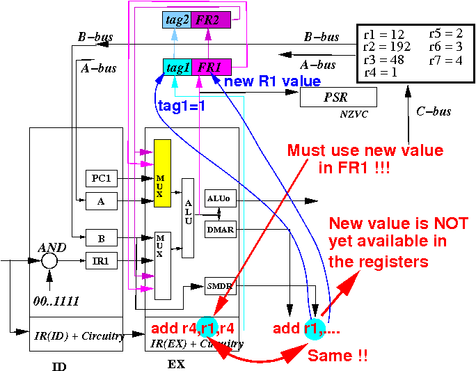
The
read-after-write data hazard
caused
by an
ALU instruction
|
Solving the
read-after-write data hazard
caused
by an
ALU instruction
Solution: we add a short-cut to allow the ID stage to fetch the new value(s) ASAP
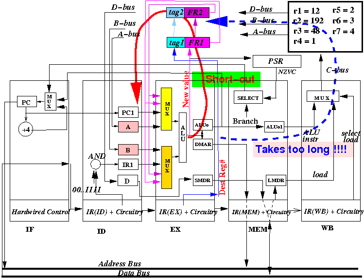
The short-cut solution is called: data forwarding
Circuitry to implement the
data forwarding technique
The circuit that implements the data forwarding technique is as follows:
Tag register stores the register number of the register being updated
Forwarding register stores the new value of the (updated) register
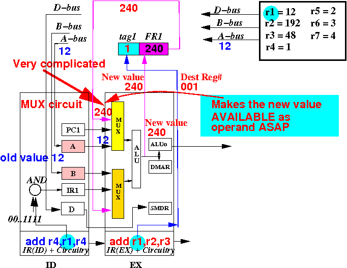
The data-forwarding technique
(i.e.: how to make a short-cut)
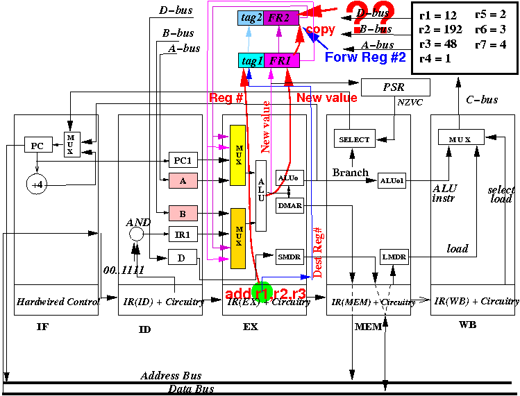
The relevant part of the CPU in the basic pipelined CPU:
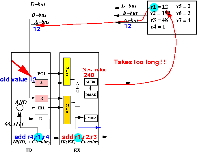
Due to delay in updating register R1, the new value cannot be fetched by the next 2 instructions
The data-forwarding technique
(i.e.: how to make a short-cut)
To make the new value available quickly, we make a copy in a reg FR1 nearby the EX stage:
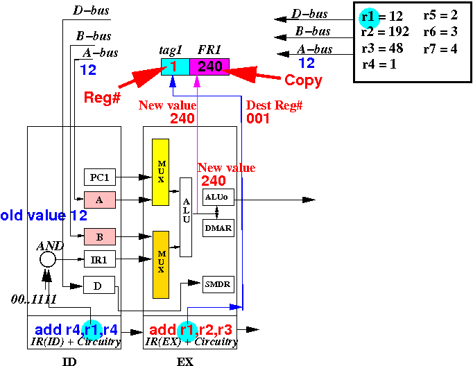
We also record the register number using the tag1 register (to identify the register)
The data-forwarding technique
(i.e.: how to make a short-cut)
The copy in FR1 is fed into the MUX so the new value can be used as operand for next instr:
Note: the MUX that selects the operand will be more complicated (discussed later !!!)
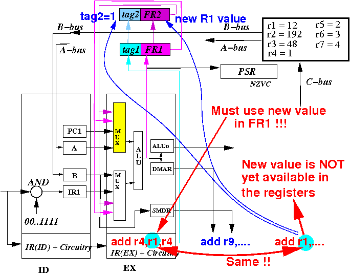
The data-forwarding technique
(i.e.: how to make a short-cut)
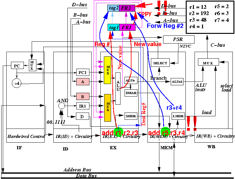
We retain the new value for another clock period by copying FR1 to another register FR2:
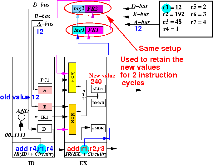
The tag1 value and FR1 value are copied to the tag2 register and FR2 register at each clock
The data-forwarding technique
(i.e.: how to make a short-cut)
The copy in FR2 is fed into the MUX so the new value can be used as operand for next instr:
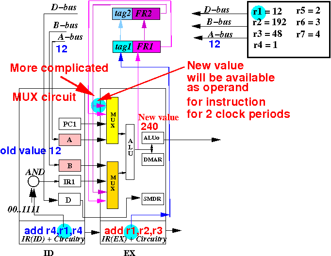
Note: the MUX that selects the operand will be even more complicated (discussed soon !!!)
The data-forwarding technique
- Summary
(1) The new value and reg # updated by the EX stage is stored in FR1 and tag1 registers
(2) The content of Forwarding Register #1 is copied to Forwarding Register #2
The data-forwarding technique
- Quiz
What is stored in the tag2 and FR2 registers ???
Hint: this was the content of tag1 and FW1 registers in the previous clock cycle !!!
The data-forwarding technique
- Quiz answer
What is stored in the tag2 and FW2 registers ???
The register number and new value produced by the instruction that is now in the MEM stage !!!
The data-forwarding technique
- Quiz answer
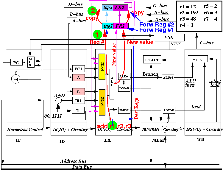
What is stored in the tag2 and FW2 registers ??? Example:
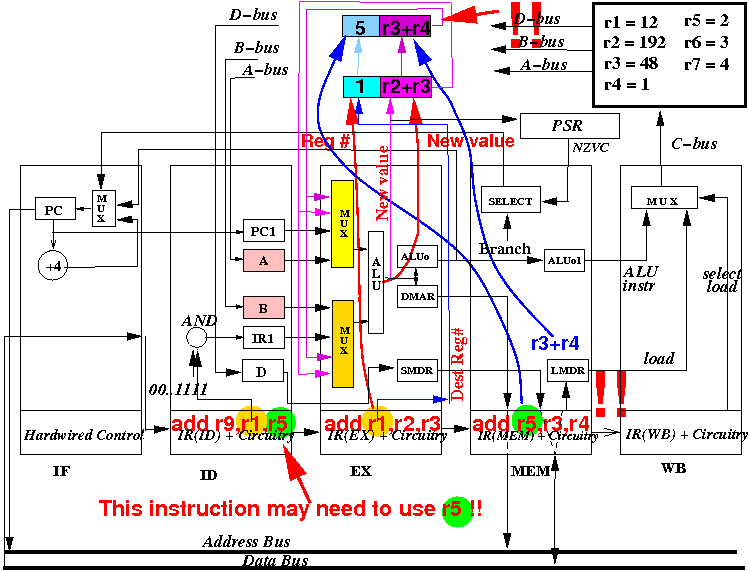
The new values are retained for 2 clock periods so the instruction in the ID stage can fetch them
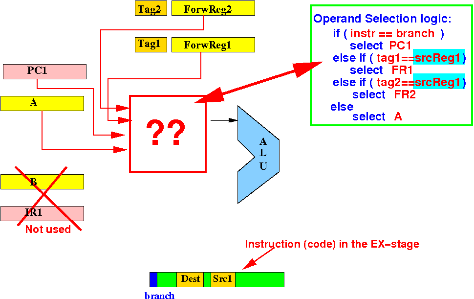
What must the operand selection Multiplexors
in the EX-stage do ?
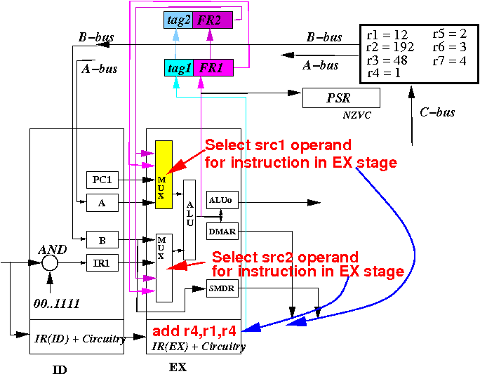
The Multiplexors in the EX-stage are used to select the correct operand for the instruction:
What must the operand selection Multiplexors
in the EX-stage do ?
Fact 1: the new value of the prior instruction is in (tag1 and) FR1 register:
Therefore: if we detect that the instruction in EX stage uses the new value, we must select it !!
What must the operand selection Multiplexors
in the EX-stage do ?
Fact 2: the new value of 2 instruction prior is in (tag2 and) FR2 register:
Therefore: if we detect that the instruction in EX stage uses the new value, we must select it !!
What must the operand selection Multiplexors
in the EX-stage do ?
How do we make these operand selecting multiplexors:
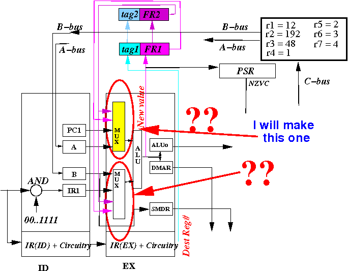
I will design the upper operand selection multiplexor - you can design the lower one similarly.
What must the operand selection Multiplexors
in the EX-stage do ?
The operand selection logic for the upper selection circuit is as follows:
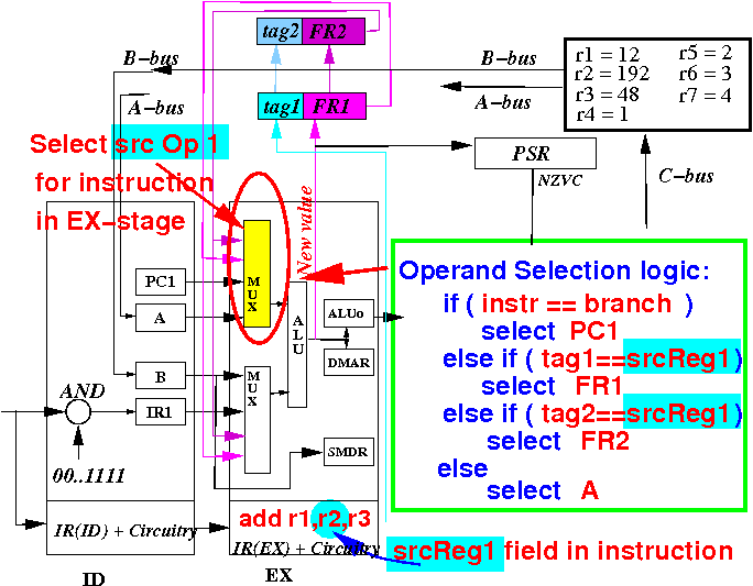
We will construct this (nested) if-expression in digital circuits !! (Logic expressions can be constructed in software or hardware !)
Constructing the operand selection multiplexor 1
The operand selection logic is:
Constructing the operand selection multiplexor 1
This multiplexor controlled by a branch instruction detection circuit:
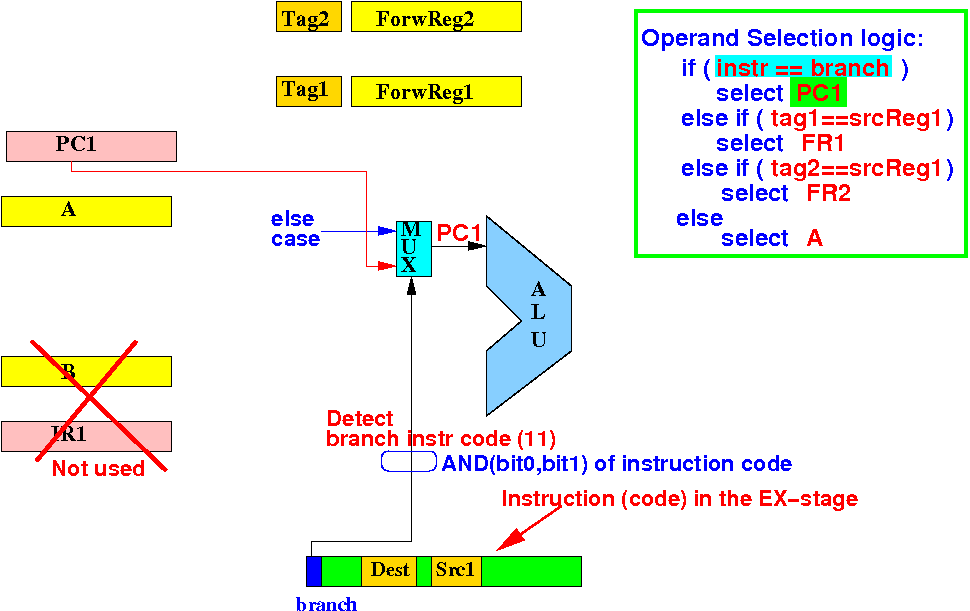
will select the PC1 register as src operand 1 for branch instructions
Constructing the operand selection multiplexor 1
This multiplexor controlled by the tag1==srcReg1 detection circuit:
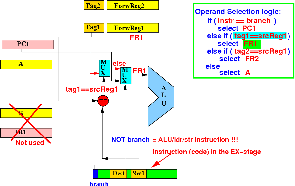
will select the FW1 register as src operand 1 for a ALU/ldr/str instruction
Constructing the operand selection multiplexor 1
This multiplexor controlled by the tag2==srcReg1 detection circuit:
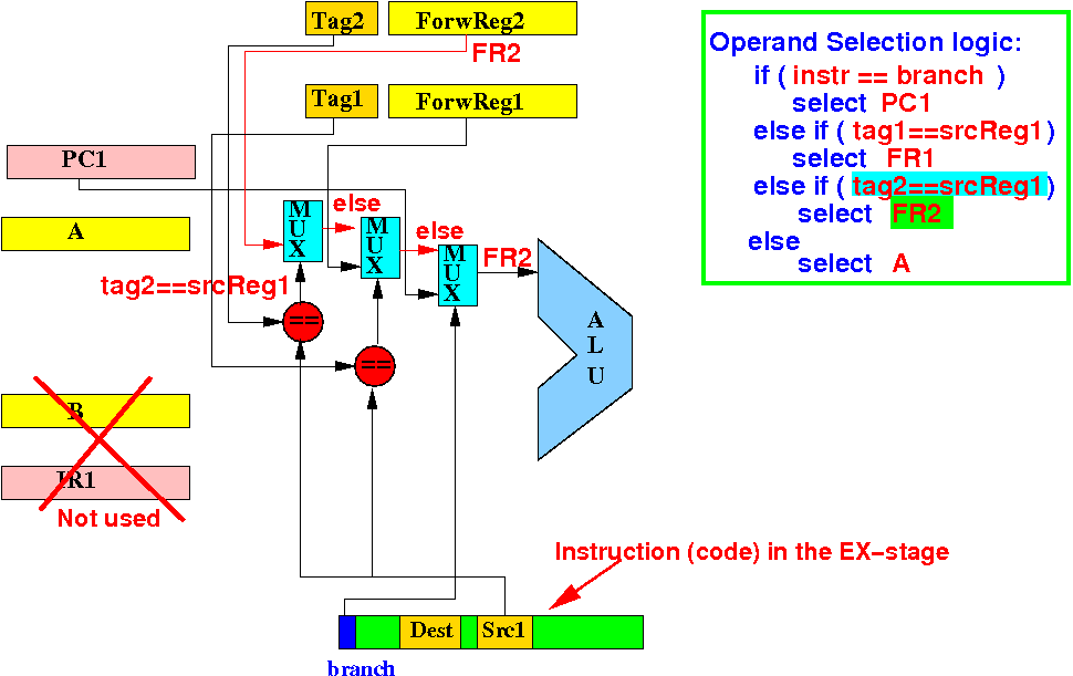
will select the FW2 register as src operand 1 for a ALU/ldr/str instruction
Constructing the operand selection multiplexor 1
If all cases fail, we can safely use register A as scr operand 1 for the instruction:
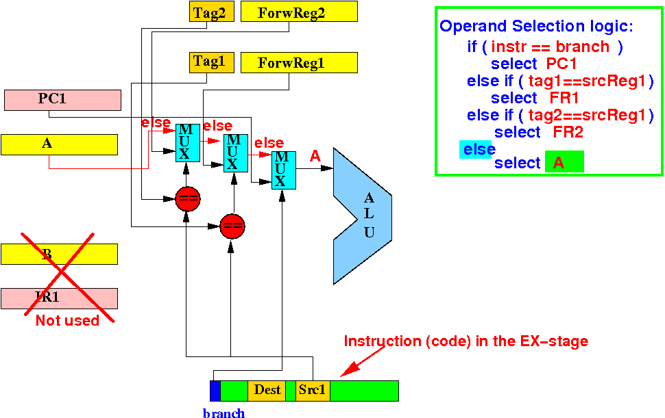
will select the FW2 register as src operand 1 for a ALU/ldr/str instruction
Constructing the operand selection multiplexor 2
to select source operand 2
The operand selection logic for the lower selection circuit is as follows:
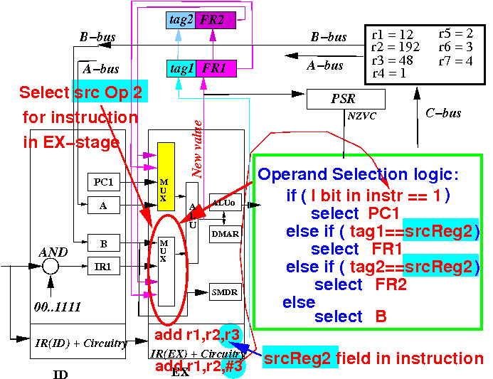
This circuit is similar to the upper selection circuit (so I will not draw out the circuit diagram)
The == compare circuit
We still have one circuit left that need explaining/designing:
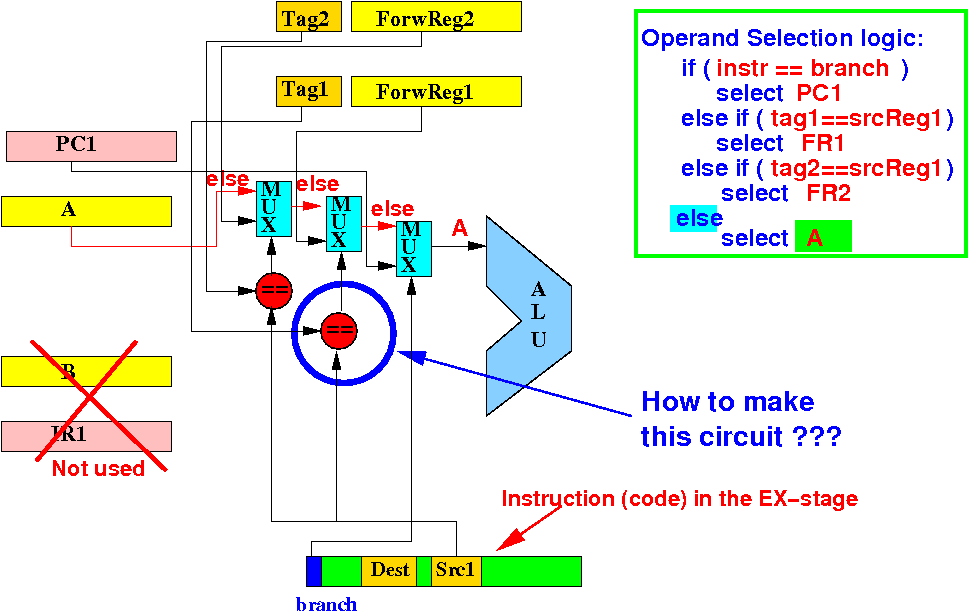
This == circuit outputs 1 when both input (binary) numbers are equal and 0 otherwise
Constructing the == comparison
circuit
The function of the == comparison circuit:
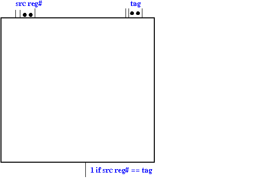
The == circuit outputs 1 when src reg# == tag amd outputs 0 otherwise
Constructing the == comparison
circuit
We compare one bit at a time: circuit:
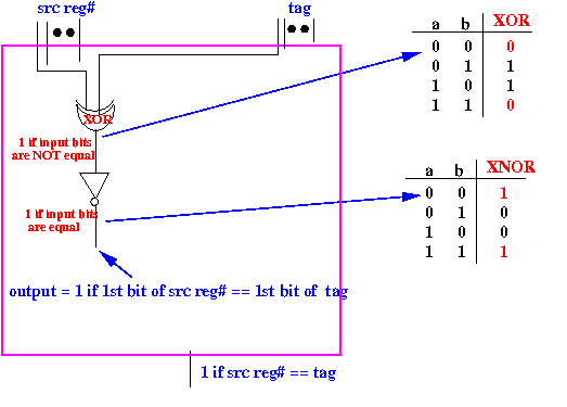
XNor(x,y)=1 if and only if bit x == bit y
Constructing the == comparison
circuit
We compare the 2nd bit of the input numbers: circuit:
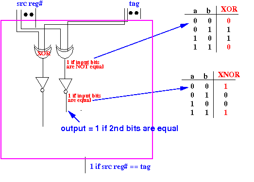
The 2nd output = 1 if the 2nd bits in the input numbers are equal
Constructing the == comparison
circuit
And so on... We compare the last bit of the input numbers: circuit:
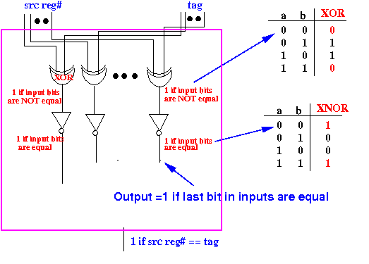
The last output = 1 if the last bits in the input numbers are equal
Constructing the == comparison
circuit
The == comparison circuit is then as follows: circuit:
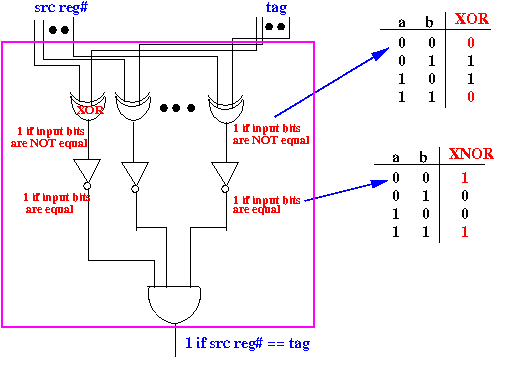
The output = 1 when all bits in the input numbers are equal