- registers
- memory
The CPU can write the result of the operation to:
- register
- memory
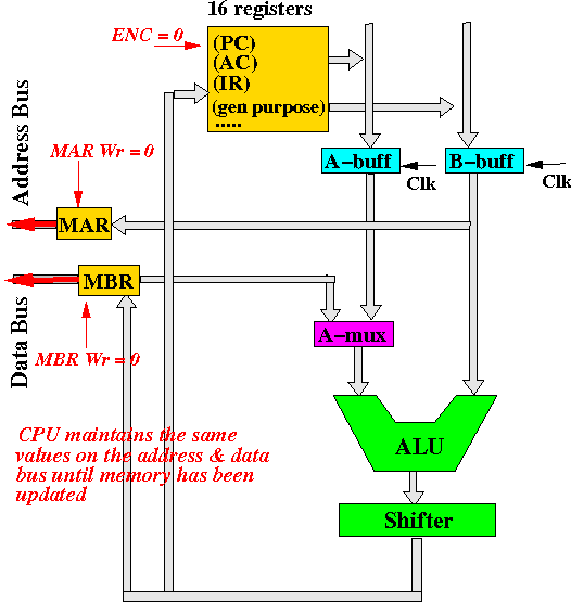
The following figure summarize the control signals (they are given in red:
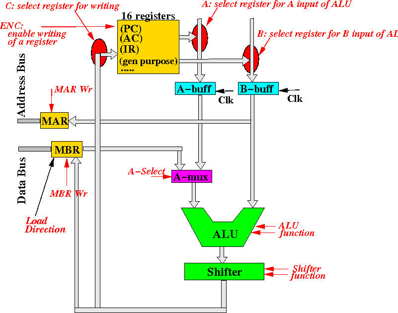
- A: (4 bits) select the register whose output will be used as the A-input
for the ALU [How: use multiplexors]
- B: (4 bits) select the register whose output will be used as the B-input
for the ALU [How: use multiplexors]
- C: (4 bits) select the register for update.
Note: the selected register is only updated if the ENC signal is ONE. - ENC: enable update of some register.
Some instructions do not update registers, like the CMP (compare) instruction (sets flags). The ENC signal will allow the CPU to specify that no registers will be updated. - A-select: controls a set of multiplexors that select the input between
a register or the MBR.
If A-select = 0, the A-MUX multiplexor will select the register as output. And if A-select = 1, the A-MUX multiplexor will select the MBR as output.
By selecting the input from the register, the CPU will perform operations on register data.
By selecting the input from the MBR, the CPU will perform operations on memory data. - ALU function: selects the function that the ALU will perform
(00 = add, 01 = and, 10 = first operand, 11 = not first operand,
as given in Prject 3
- Shifter function: selects the function that the Shifter will perform
(00 = no shift, 01 = shift right, 10 = shift left,
as given in Prject 3
- MAR Write: trigger the MAR (Dffs) to be updated.
Note: by looking at the connections, you must conclude that the MAR will be updated with the value in the B-buffer - MBR Write: trigger the MBR (Dffs) to be updated.
Note: by looking at the connections, you must conclude that the MBR can be updated with data from:
- C-bus (output of the Shifter)
- Databus (data from memory)
In a read operation, data from the databus is first transfered into the MBR. In this case: MBR is updated with data from the databus). After the memory data reaches the MBR, it will be further transported to its final destination through the datapath.
In a write operation, data from a register is first transfered through the datapath into the MBR. In this case: MBR is updated with data from the C-bus (shifter output). After the memory data reaches the MBR, it will be further transported to its final destination through the databus to the memory.
- Load direction: control whether the MBR will be updated with
data from memory or with data from the C-bus.
Note: you have see enough examples where the CPU need to pick 1 thing among N things that you need to use a multiplexor. In case you still don't have any idea how the CPU picks among the databus and C-bus input, Project 7 will spell it out for you....
- Register to register operation:
- Operands are fetched from registers
- Result is written to a register
The following figure shows the pathway of the data flow in a "register-to-register" operation through the simple datapath and how this type path is setup in our simple CPU:
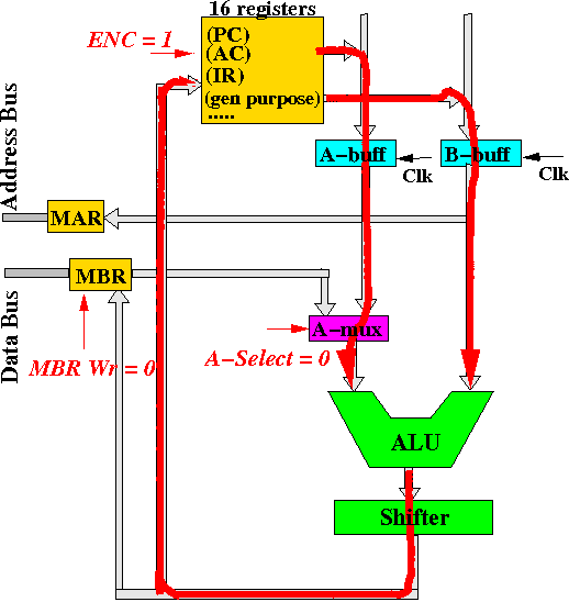
Notice the setting of the control signals on the datapath to effectuate a register-to-register operation:
- A-select = 0, so that data from a register is forwarded to the ALU
- ENC = 1, so some register is updated.
- MBR-write = 0, so that MBR is not updated
Example of such operations:
- MOVE R1, R2
- ADD R1, R2, R3
- NEG R1
- Memory read operation:
- at least one source operand data is fetch from memory
- CPU first sends out the address of the memory operand
- the data is fetched into the MBR
- the result (for simplicity) is written to a register in the CPU
Note that the data from memory is always first fetched into the MBR and then transfered to the final (register) destination. The following 2 figures show that data from memory is transfer into a register of the CPU in our very simple datapath:
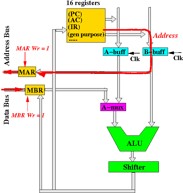
- First, the CPU outputs the address
of the memory to obtain the data.
To do this, the CPU must update the MAR register with the
desire address. The only way to do so is to send out the address from
some register on to the B-bus and set the MAR write signal to 1
to trigger writing of the MAR.
- Now the address is on the address bus and the CPU must send out
an "Memory Read" instruction on the system bus.
We will see how this is done in more details later in the course,
but for now, you only need to know that after some time (because
the speed of light is finite) the data from the memory will
be available on the data bus
- At the proper moment, the CPU will trigger a MBR-write signal so that the data on the databus will be written into the MBR.
After the data from memory has been written into the MBR, the data will be moved to its final destination (which is always a register inside the CPU) through the datapath with the setting given in the following figure:
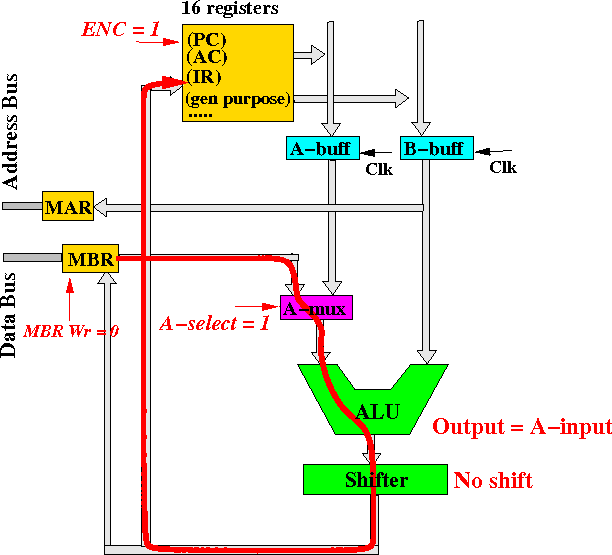
Notice the setting of the control signals on the datapath to effectuate this transfer is:
- A-select = 1, so that data from MBR is forwarded to the ALU
- ENC = 1, so some register is updated.
- MBR-write = 0, so that MBR will keep (= remember) its value
- Memory write operation:
- data from a register is written to a memory location
- CPU sends out the address of the memory
- CPU sends out the data to the memory
- CPU waits until the result is written to the memory
Note that the data from the CPU is always first fetched into the MBR and then transfered to the final (memory) destination. The following 2 figures show that data from register is transfer to the memory in our very simple datapath:
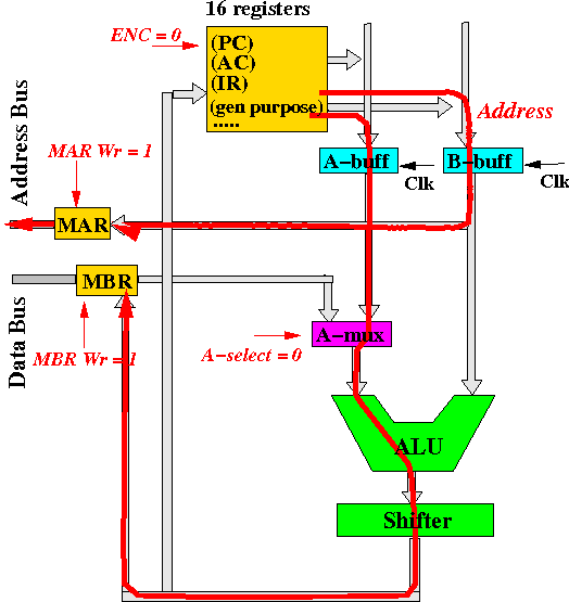
- The CPU must output the address
of the memory to write the data.
To do this, the CPU must update the MAR register with the
desire address. Again, the only way to do so is to send out the address from
some register on to the B-bus and set the MAR write signal to 1
to trigger writing of the MAR.
- The CPU must also send the data to the memory by putting
the data into the MBR.
To do this, the CPU must update the MBR with a register.
If you look at the connections carefully, the only way to
do that is through the A-bus connection.
Notice the setting of the control signals on the datapath to effectuate this transfer is:
- A-select = 0, so that data from register is forwarded to the ALU
- ENC = 0, so no register is updated.
- MBR-write = 1, so that MBR is update with A-bus register data
- MAR-write = 1, so that MAR is update with B-bus register data (which must be the address of the memory)
After the address has been written into the MAR and the data from memory has been written into the MBR, the CPU must wait until the memory has "acknowledged" that the memory location has been updated. This will be discussed later:
