Previously, we studied this (simple) data path:
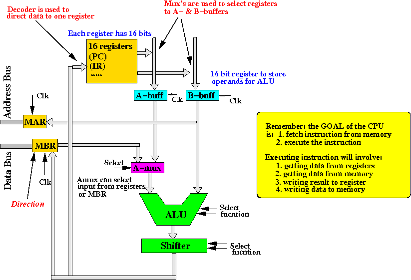
The data path is controlled using various signals:
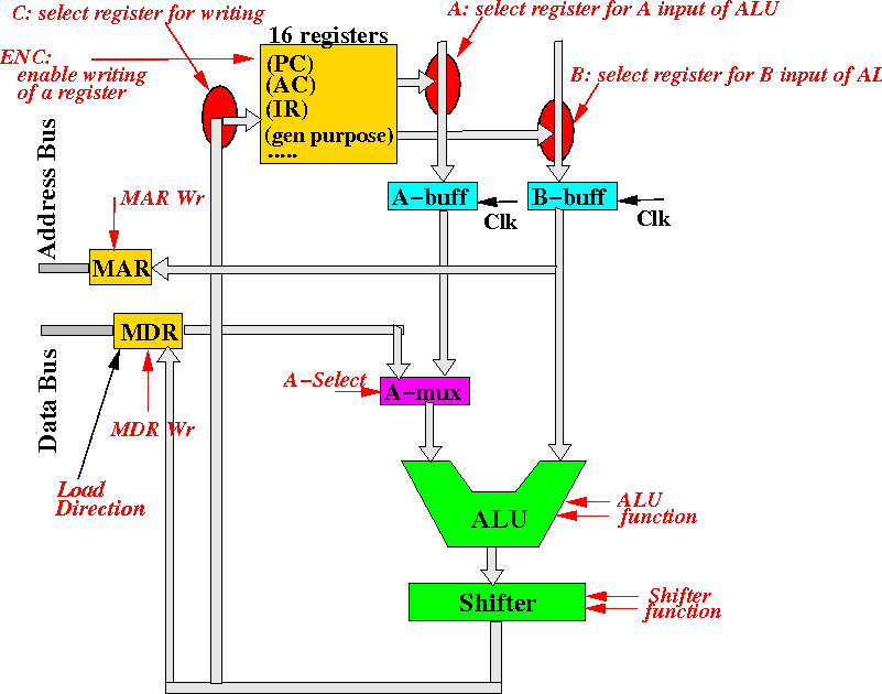
We will go over the signals one at a time next...
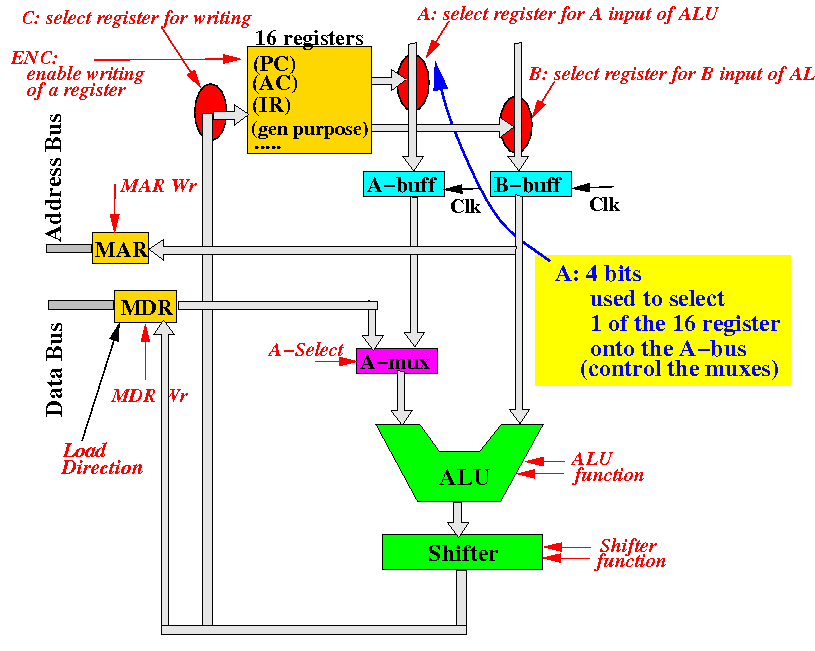
The 4 bits named A controls the multiplexors that select one of the 16 registers into the A-bus:
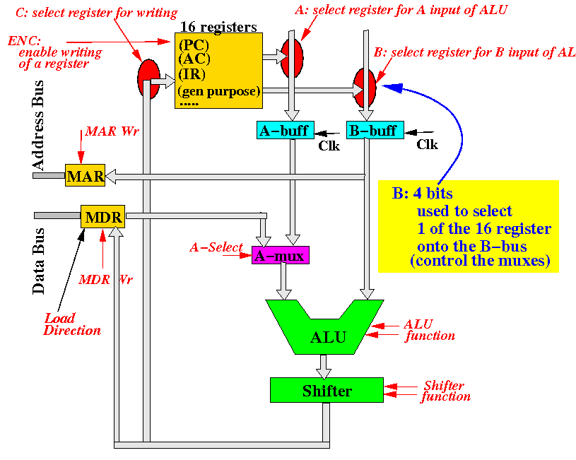
The 4 bits named B controls the multiplexors that select one of the 16 registers into the B-bus:
The 4 bits named C controls the decoder that select one of the 16 registers for writing:
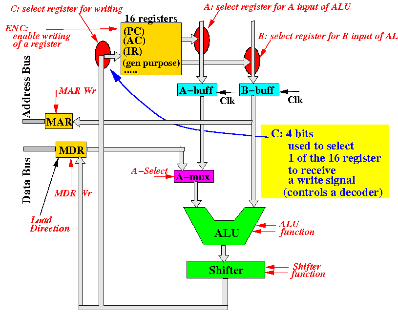
The 1 bit named EnC controls whether or not a register will be written:
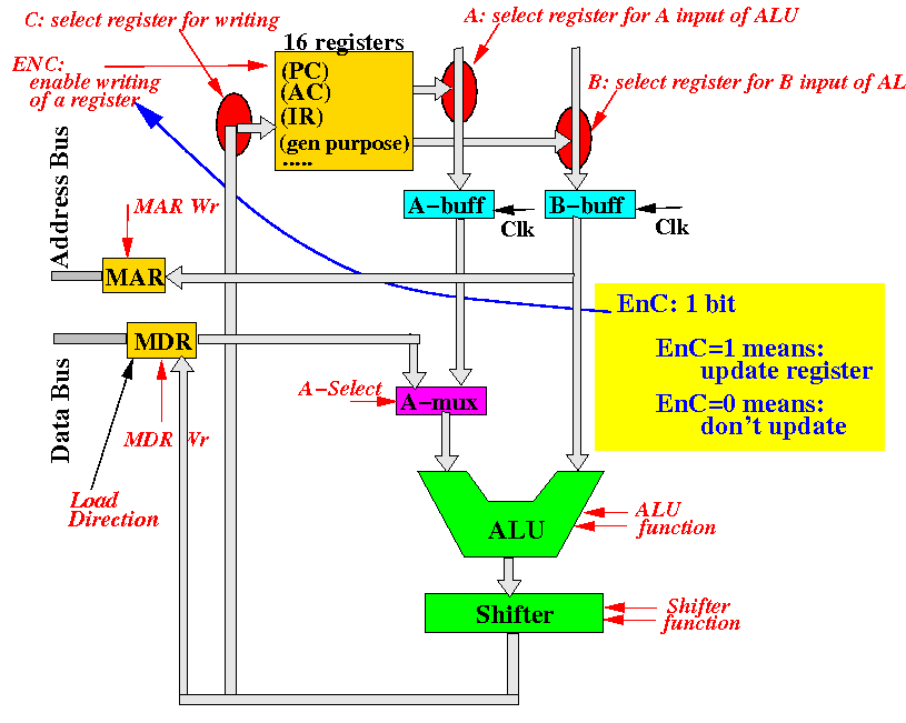
The 1 bit named A-Select controls the selection between MDR output and A-bus as first input of the ALU:
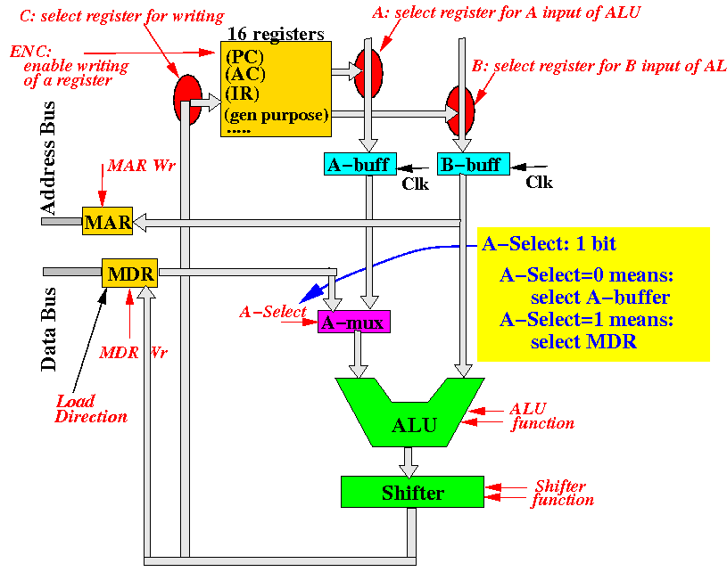
The 1 bit named ALU controls the operation that the ALU will perform (= part of the opcode)
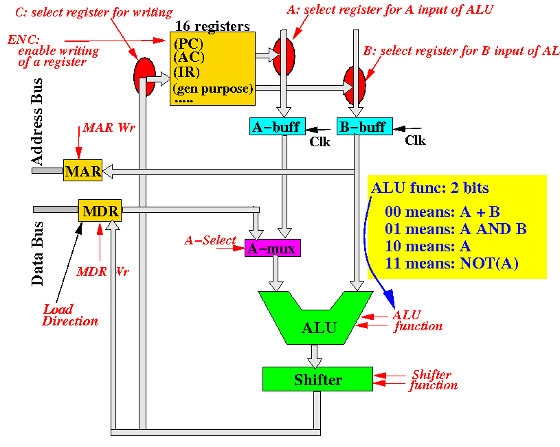
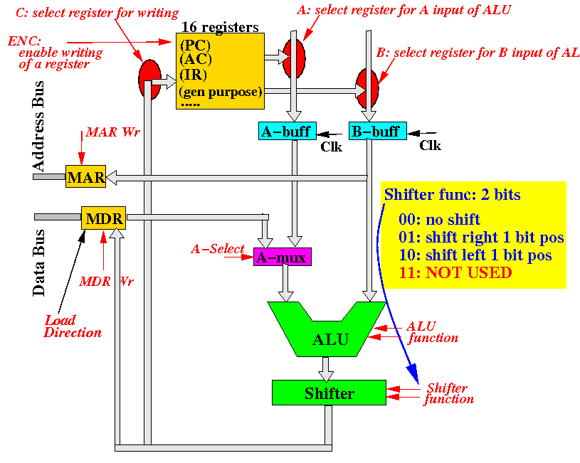
The 1 bit named SHF controls the operation that the shifter will perform (= the other part of the opcode)
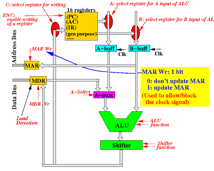
The 1 bit named MAR Wr controls whether or not the MAR register will be written:
The 1 bit named MDR Wr controls whether or not the MDR register will be written:

|
The instruction format of the simple CPU that we will build:
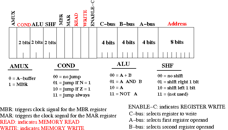
Note: we will not use (nor discuss) the signals given in red in the diagram above...
Bits in the IR are connected to the selection device (e.g.:mux) that it controls on the datapath:
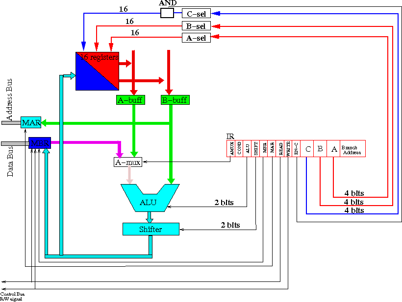
Example: the field A (= source operand 1) in the machine instruction
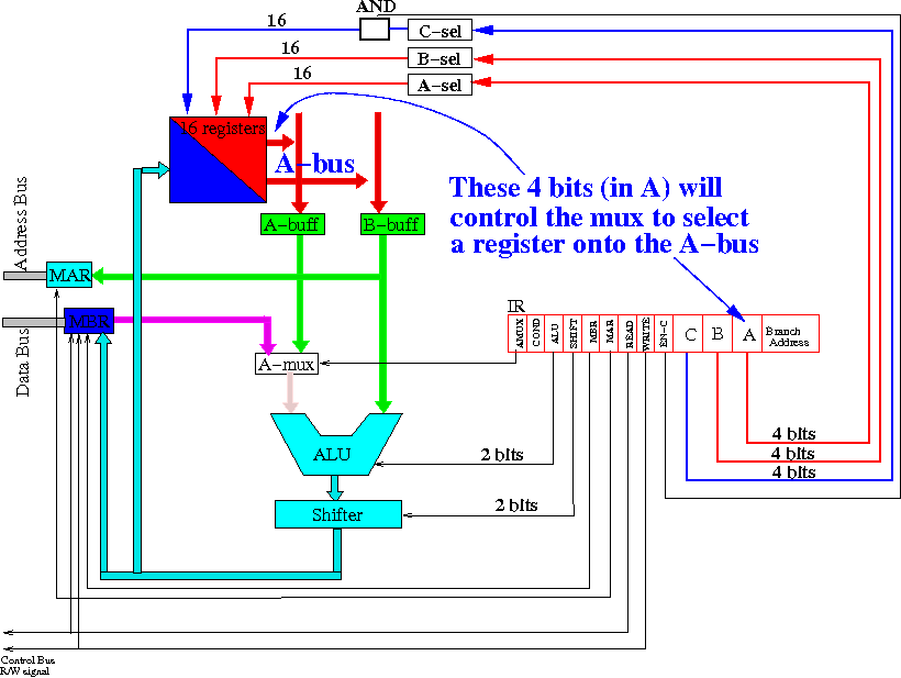
Example: the field B (= source operand 2) in the machine instruction
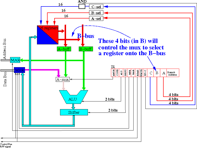
Example: the field C (= destination operand) in the machine instruction
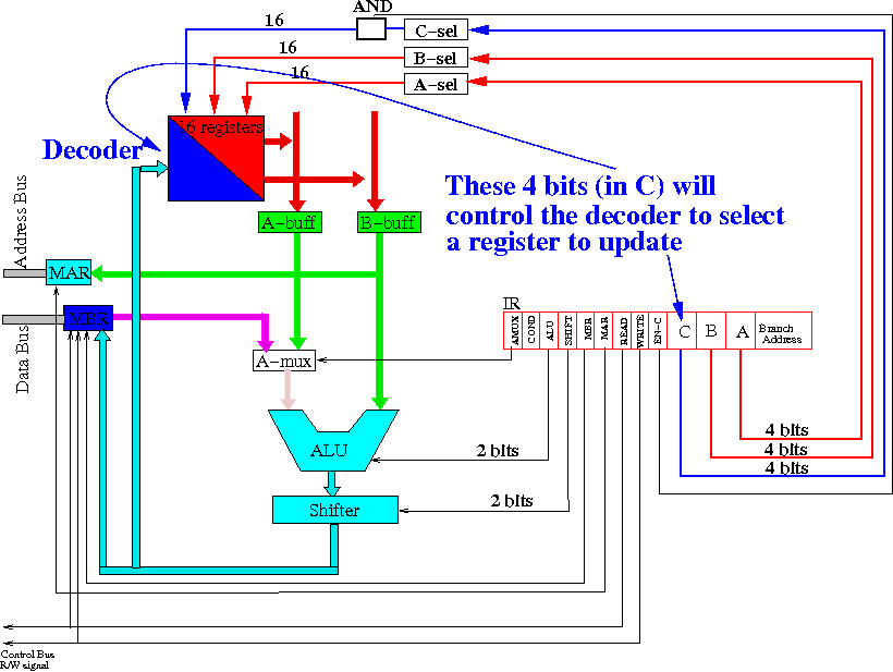
Example: the fields ALU and SHIFT (= opcode) in the machine instruction
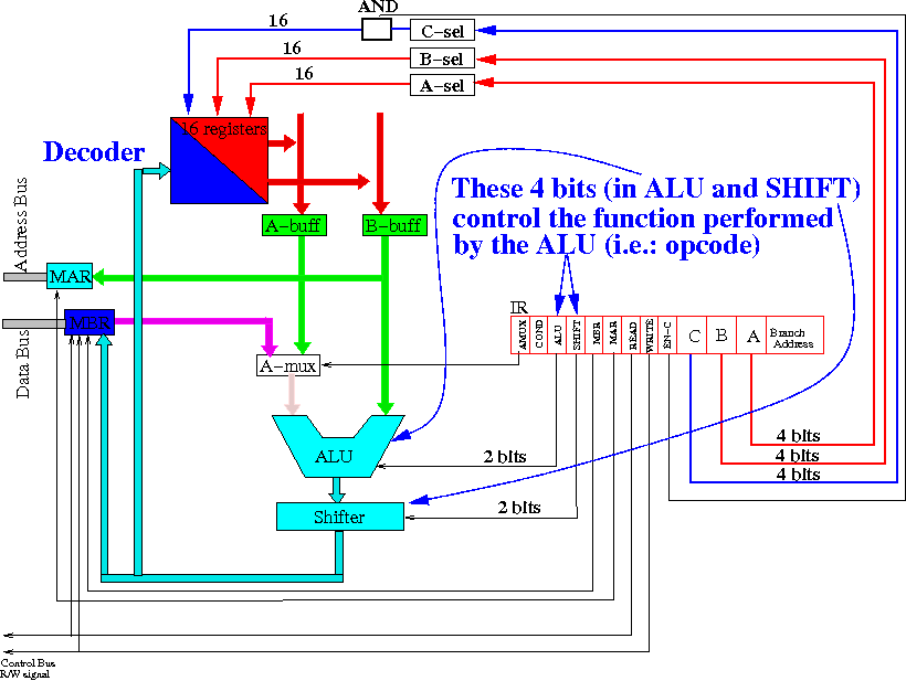
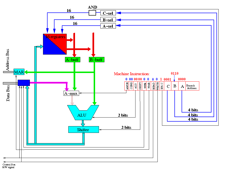
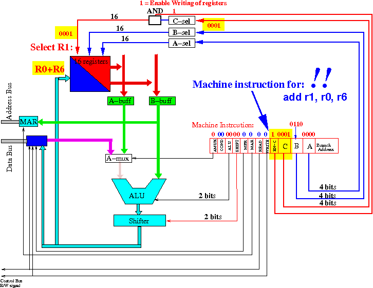
Sample machine instruction: (see binary number inside IR)
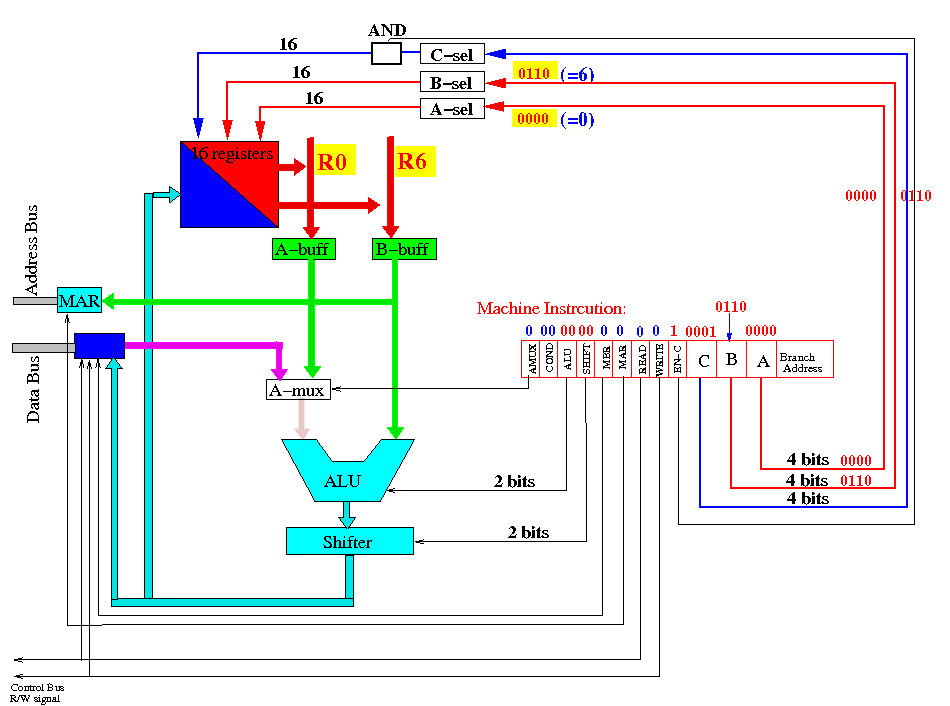
The A-field and B-field will forward R0 and R6 onto the A- and B-buses:
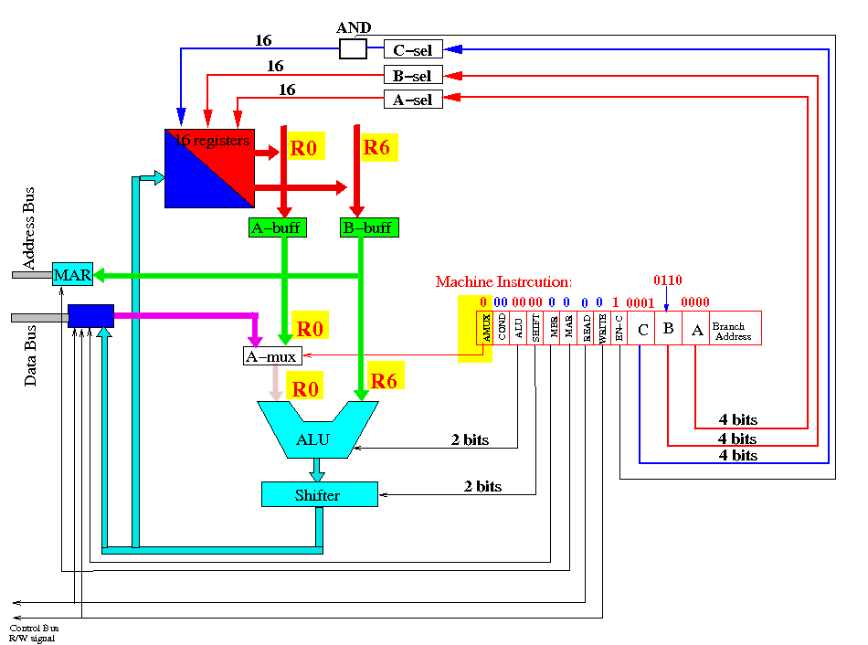
The AMux bit will select data from the A-bus to be forwarded to the ALU input:
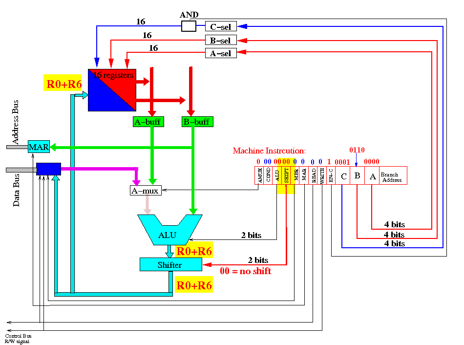
The ALU and SHIFT bits will select the ADD and NO SHIFT operations:
The C and EnC bits will update the register R1 with the output value from the ALU:
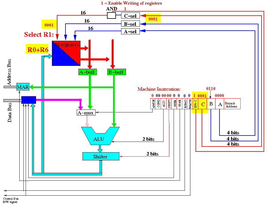
In other words, the machine code instructs the CPU to perform: add r1, r0, r6 !!!
|