|
DEMO on what I meant: /home/cs355001/demo/circuits/1-bit-memory
From the demo, we can construct the logic table of the 1-bit memory circuit:
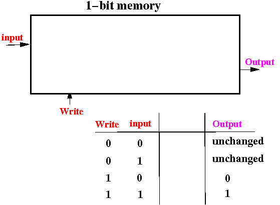
The logic table describes the behavior of the 1-bit memory circuit unambiguously
We can use the SR-latch as memory retention circuit to store 1 bit:
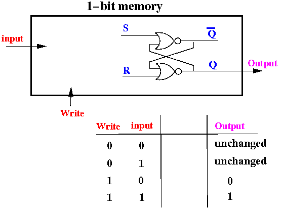
We will adapt the SR-latch to operate in the "more suitable" way that we want !
We can adapt the SR-latch by using a translation circuit:
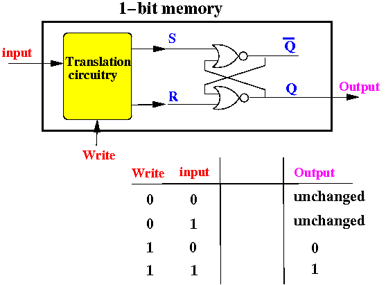
The translation circuit will translate the meaning of the (Write, Input) signal values to the appropriate (S,R) signal values !!
When (Write=0, input=0/1), we want the output to remain unchange:
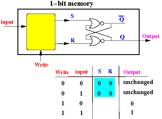
The correct values for (S,R) are therefore: (S=0, R=0) (see table)
When (Write=1, input=0), we want the output to be equal to 0: (= stores the input value)
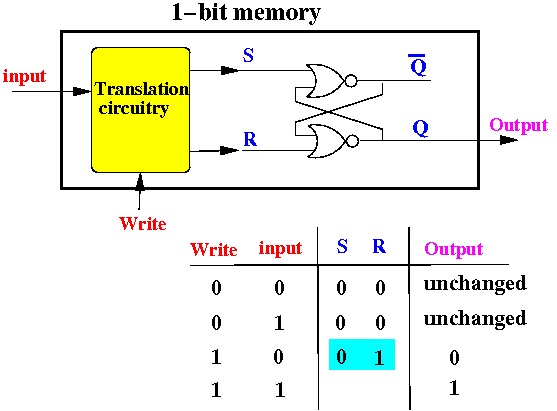
The correct values for (S,R) are therefore: (S=0, R=1) (see table)
When (Write=1, input=1), we want the output to be equal to 1: (= stores the input value)
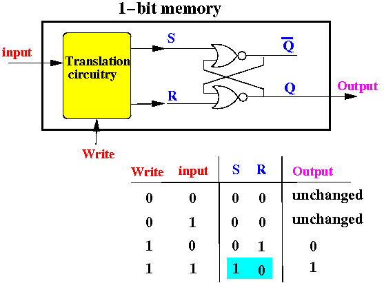
The correct values for (S,R) are therefore: (S=1, R=0) (see table)
The logic table for the translation circuit is:
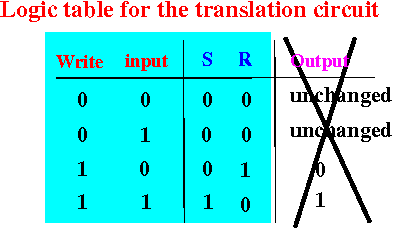
We could use the "good old" circuit design method to construct this translation circuit...
But the circuit is very
simple:
S = Write AND input
R = Write AND
(NOT input)
Final result:
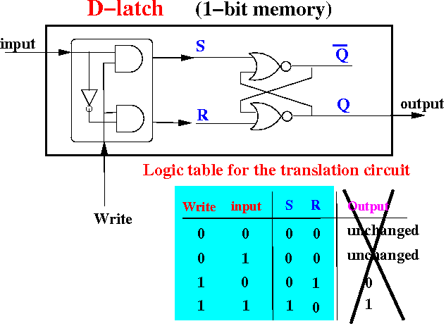
This digital circuit is called the D-latch
DEMO: /home/cs355001/demo/circuits/d-latch
A 4-bit memory circuit is constructed with 4 D-latch circuits controlled by the same write:

Note: the
write signal is
called the
clock signal in
digital electronics
DEMO:
/home/cs355001/demo/circuits/4-bit-memory
Recall when I discussed the decoder, I explained the functionality of the D-latch:
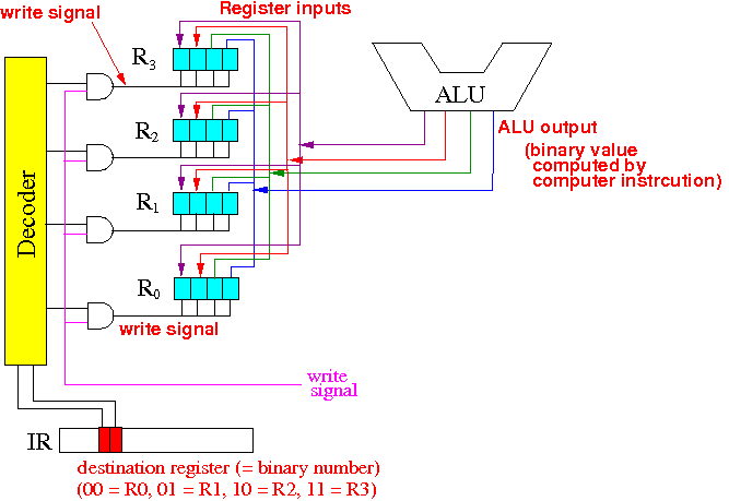
A set of D-latches
(= a register) will be
written by the
write signal controlled by the
decoder circuit
DEMO:
/home/cs355001/demo/circuits/alu-reg
